Whats inside?
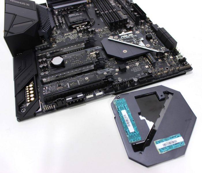
First thing I did was lay the board out and start pulling the covers to see what lies underneath.
Here you can see the PCH heatsink cover and its affixed thermal pads. These thermal pads are in place as the PCH Heatsink cover also covers the two M.2 slots mentioned previously and acts as a thermal sink for high-speed drives if they are placed in the DMI connected slots.
Here we now remove the VRM heatsink and as you can see the heatsink is more than beefy along with being heat pipe connected to help spread the load although with the VRM this board is equipped with it should run rather well under any normal loading scenario. We also noted a thermal pad which is at the far edge and had some creases in it. There is a supplementary cooler under the IO cover which we will be pulling off.
After everything is removed we get a clear view of the VRM components. First of note is the VRM controller and components themselves. The controller is listed as ASP1405i which i am quite certain is just a rebranded International Rectifier IR35201. This is an 8 phase digital contro9ller which can run at 8+0, 7+1 or 6+2. This is a very competent controller used across many top end boards and with the ASUS “10 Phase” CPU VRM we can be assured it will easily feed more than enough to push your 9900K to its limits. Theoretically, the VRM on the Extreme board should handle in excess of 600Amps which is simply unrealistic as even under the most extreme cooling such as Liquid Helium I don’t see you getting to that power draw.
The power stages are International Rectifier IR3555M units which are capable of up to 60A hence the previously mentioned 600A top end. Now obviously this does mean that in normal operation this VRM will stay in a very nice efficiency range simply not pumping too much heat even when under load as the 200A at an estimated maxed out 9900K on standard ambient cooling would be approximately 20A per phase which would mean likely less than 15W total dissipated which could be cooled passively without a heatsink at all. This VRM is a shining example of overbuilt.
The supplemental cooler we saw before once removed we sound it is used for cooling the Aquantia AQC111C which is the controller for the 5G LAN.
Next up for the IC’s feeding the REAR IO as well would be an ASMedia ASM1442K which feeds the HDMI on the REAR IO.
Lastly would be the ASMedia ASM1464 which is used to feed some of the USB 3.1 Gen 1 (5Gbps) ports.
 Bjorn3D.com Bjorn3d.com – Satisfying Your Daily Tech Cravings Since 1996








I seem to be having a bit of a situation with this board and I thought you might be able to help. It would seem that somewhere I’m not sure if it’s in the Bios or if it’s on the board that for an m.2 slot there’s a switch between usb and pcie. Currently mine is at usb and I would like to change it pcie.
Thanks if you can help.
Also I was wondering if I upgrade the BIOS does it change all the settings back to default?
Normally I would save a BIOS profile before flashing and set it to defaults to relieve the variable which may cause a bad flash.
Also, there is no USB signal at all going to an M.2 slot, can you please further explain what you are referring to?