The Ivy Bridge promises higher performance per watt over Sandy Bridge on both the CPU and GPU front. Built with tri-gate 3D transistors on a 22nm die, how much performance should we expect from the new CPU?
INTRODUCTION
The 7 series chipset, launched on April 8 set the ball rolling for the launch of the Ivy Bridge, the die shrink to Sandy Bridge. Finally, after a bit of delay, we get a look at the highly anticipated third generation Core processor from Intel.
If you have been following Intel products over the last few years, you should be familiar with the company’s yearly product launch cycle which they called the tick-tock model. In this model, a new microarchitecture (tock) is launched, followed the next year by a die-shrink of the same microarchitecture with minor improvements and performance enhancement (tick). Following this model, Intel has been able to keep delivering new products yearly since 2008.
Often with the tick, Intel tweaks existing microarchitectures to enhance the overall performance while lowering the power consumption with the help of a die-shrink. However, this time with the Ivy Bridge, Intel has done more than just minor tweaks. Ivy Bridge brings us not just a faster performance CPU at lower power consumption, thanks to the 22nm, it also brings the a major GPU upgrade, with the first DirectX 11 GPU from Intel. Since Ivy Bridge is more than just minor tweak, Intel called this launch as “tick+”, giving us a major microarchitecture change on the GPU along with minor CPU enhancement.
Looking at the Intel Ivy Bridge Press Deck, we get a feeling that many features on the Ivy Bridge are designed with mobile platforms in mind as many of the new tweaks are aimed to lower the systme power consumption. Ivy Bridge is designed to keep the same level of performance as Sandy Bridge while bringing the power consumption even lower. This makes sense as the computing landscape has changed over the last few years: light, portable laptops have gained ground in favour of bulky, stationary desktops. Thus, by reducing power consumption and focusing on improving performance per watt than just raw performance, Intel is able to design a chip that can be more equally efficient in either a desktop or a laptop.
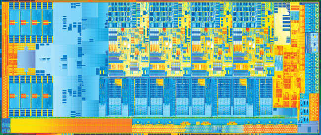
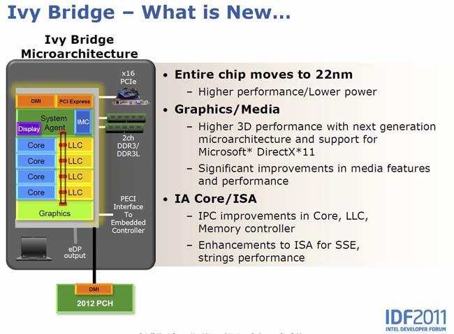
The Ivy Bridge die (source Intel)
The Sandy Bridge architecture has 1.16 billion transistors packed in a 216 mm2 die area. Ivy Bridge, in comparison, has a smaller die of 160 mm2 but more transistors (1.4 billion). Thanks to the 22 nm fabrication process, Ivy Bridge has significantly reduced its die size so despite containing more transistors, it is smaller. For Ivy Bridge, the extra transistors primarily go to the GPU since there are same number of cores and cache on both processors.
CPU IMPROVEMENTS

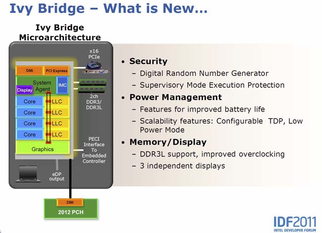
Ivy Bridge’s CPU portion is not very different from Sandy Bridge. The processor contains the CPU cores, graphics, media and display engine, memory controller, PCI Express controller modular on-die ring interconnect, and shared low-level cache (LLC). The maximum number of cores is still four, with some models supporting HyperThreading. The quad core Ivy Bridge CPUs will have up to 8MB of L3 cache; the L1 cache still remains at 32+32K and the L2 cache is still at 256K.
While the official memory speed on the controller is still 1600MHz (the same as Sandy Bridge), Ivy Bridge has a DDR ratio/frequency up to 2667MHz (up from 2133MHz on the Sandy Bridge and 2400MHz on the Sandy Bridge-E). The memory can now be increased in either 200 MHz or 266 MHz increments. In addition to regular DDR3, the mobile Ivy Bridge will support low voltage DDR3 (DDR3L) that operates at 1.35V (as opposed to standard DDR3, which operates at 1.5V).
Intel has also made a few tweaks to the CPU unit to make Ivy Bridge faster. The Ivy Bridge has a few improved IA Core/IS, improved memory controller, and a cache system that helps to improve the IPC and the graphics performance. Among the improvements in the instruction set architecture (ISA) are:
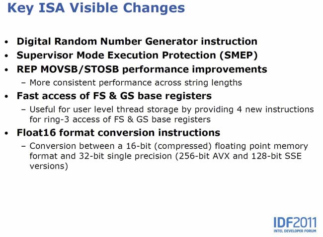
The Ivy Bridge’s resource allocation to HyperThreading has also been improved. If there is a single thread active, all of the resources will be dedicated to that thread. This should be very useful particularly in dual-core models, as it will improve single-threaded performance and also helps to reduce the power consumption.
The fast access of FS and GS base registers enhances server workloads, resulting in improved user-level thread storage. The Float16 format is an extension of the AVX instruction set on the Sandy Bridge. This is a format conversion between the compressed 16-bit float point to the single precision format. The MOV instruction is also improved and more efficient on Sandy Bridge.
The float point/integer divider on Ivy Bridge has twice the throughput compared to the Sandy Bridge. The additional throughput from the floating point unit in particular will be very useful and should show sizeable improvement at complex calculations.
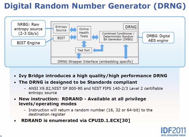
A couple of new ISA additions to Ivy Bridge are designed to increase security. The chip now includes a high quality/high performance DRNG (digital random number generator) and Supervisory Mode Execute Protection (SMEP). Available in both user and OS level code, the DRNG can generate random numbers that would be useful for security programing such as cryptography.
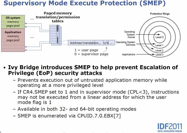
The SMEP is a hardware-level protection against Escalation of Privilege security attacks.
Based on Intel’s estimate, Ivy Bridge will have about a 5% improvement over Sandy Bridge at the same clockspeed.
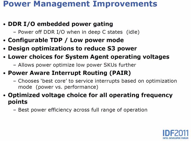
Power Management Improvements
Ivy Bridge continues to offer a high CPU performance as Sandy Bridge but at lower power consumption. It is clear that one of the main goals with Ivy Bridge is to reduce the power consumption. The fastest Sandy Bridge has a max TDP of 95W. With Ivy Bridge, Intel is able to reduce 18 watts of power and the fastest Ivy Bridge has the max TDP of 77W. Obviously, Intel is aiming to deliver equivalent or better CPU performance per watt over Sandy Bridge. This also means that Ivy Bridge should run cooler than Sandy Bridge at the same clockspeed.
Ivy Bridge is the first 22 nm processor in the world and it is built on Intel’s 22 nm 3D tri-gate transistors. The tri-gate transistor adds a new dimension to the traditional planar transistor, which allows the chip-maker to have tighter power controls on the chip so that the power consumption can be reduced and the clock frequency can be scaled better. Such a design works better at the lower end of the voltage scale: Intel claims the 22 nm process to have a 37% increase in performance over the 32 nm process, and an 18% increase in performance at 1V. What this translates to is that a 22 nm tri-gate processor can run at higher clockspeeds while consuming the same power; or it can operate at the same clockspeed at lower power consumption. With Ivy Bridge, Intel is taking the latter approach as the main goal is to reduce the overall system power consumption.
Many of the tweaks on the Ivy Bridge are designed to save power. The Sandy Bridge already has the ability to shut off individual GPU or CPU cores when they are not being used. Now with Ivy Bridge, the DDR3 interface is also gated so that it can be completely shut off to conserve even more power when the system is in deep C state (idle).
The Ivy Bridge also has optimization to reduce the S3 power which would be useful to extend your battery power, and the operating voltage is also being optimized. The System Agent is the area on the CPU that contains the display output, memory controller, DMI and PCI Express interface. In the Sandy Bridge, there are two choices of System voltages and on Ivy Bridge, the voltage has been reduced even further for low power SKU models.
Configurable TDP
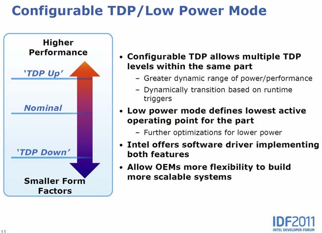
With Ivy Bridge, Intel introduced configurable TDP. Traditionally, TDP is set by processor makers, and cannot be changed. The CPU can operates at any speed under the TDP limit. With Ivy Bridge’s configurable TDP, it is possible for the CPU to operate at different TDP’s depending on the type of cooling and power requirement. If additional cooling is provided, the CPU run at higher clockspeed for additional performance. Similarly, the TDP can also be lowered (either by reducing the clockspeed or reducing the number of active cores) to fit a chip into a smaller energy footprint or to conserve battery power.
With Ivy Bridge, Intel has the traditional nominal TDP. In addition, there are two more TDP levels, one higher and one lower, than the nominal TDP. This allows the system manufacture to configure their system to meet one of the three TDP’s depending on the system configuration. Additionally, system manufacturers can even create a system that dynamically operates at TDP’s depending on the type of power/cooling. For example, it is possible to have a laptop that operates at nominal TDP when it is on battery but when it is on a dock, it will operates at the higher TDP.
The configurable TDP is specifically designed for system manufacturers and integrators to build more scalable and flexible systems, and it is not something that the end-users would be able to adjust.
Power-Aware Interrupt Routing
Ivy Bridge has a built in logic to properly route interrupt requests to an active core as opposed to waking up an idle core. Since waking up a core requires more energy than routing to an already active core, this will reduce the power consumption. However, this can potentially lower the active core’s performance. Luckily Ivy Bridge still supports the same performance prioritization as Sandy Bridge, so you can choose between either having higher performance or lower power consumption.
Optimized voltage choice for all operating frequency points
The Sandy Bridge uses three points on the voltage frequency curve to interpolate other frequencies’s voltages. On Ivy Bridge, there are multiple operating points stored on the die that can be used by the system’s power management to create a curve which can then be used to pick the most optimal operating voltages for a given frequency.
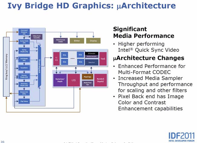
Intel HD 4000/HD2500 DirectX 11 Support
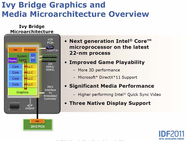
For years, Intel did not put much weight on the GPU. The firm always saw the CPU as the “central” unit in the system (after all, it is called central processing unit). However, with the advent of HD multimedia and greater graphical demands from operating systems, Intel is finally putting a greater resource on improving the performance of the integrated GPU. The Sandy Bridge architecture has a relatively capable GPU core. However, does still fall behind AMD’s counterpart in terms of performance and technology.
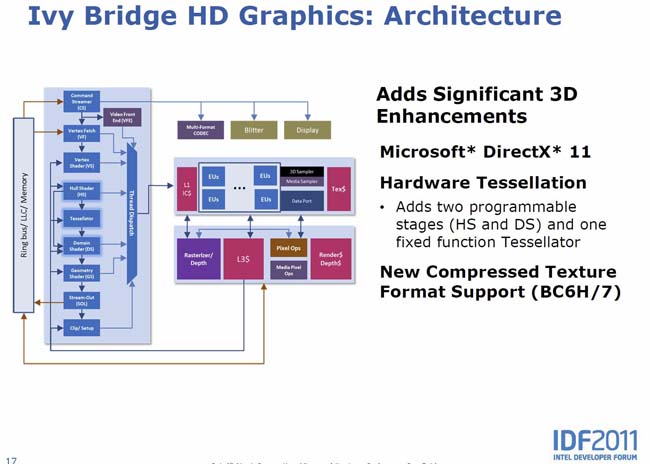
Ivy Bridge continues what Sandy Bridge started but now the new GPU adds support for OpenCL 1.1, DirectX 11 and OpenGL 3.1, putting it at the same level in terms of feature as AMD. Additionally, Ivy Bridge adds one additional display support so that it is now able to use three displays as opposed to two on Sandy Bridge. It also fully supports third generation PCI Express 3.0, which offers twice the bandwidth per lane of the 2nd generation at 8GT/s.
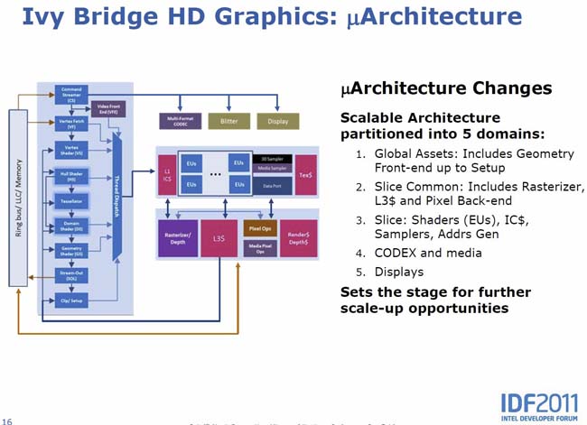
The Ivy Bridge GPU is partitioned into 5 domains.
The Global Assets (left side of the block diagram) is primarily a data flow machine. It is responsible for the geometry pipeline, Direct Compute, and breaking media and the wavefront into threads for the shader units.
The bottom right block is what Intel calls the Slice Common; it contains the rasterizer, Z-complex, stencil complex, and pixel back-end. A dedicated L3 cache is included here to store frequently used data. It is aimed to reduce the power consumption as the GPU would be able to access these data without turning the ring bus.
The middle section on the right side is the Slice Shader where we find the Execution Unit (EU), Media and 3D Sampler. The Media Sampler is responsible for image processing where the noise-reduction and de-interlacing happens. The last domain (the upper right hand corner) is the media fix functions for media encoding.
The design on the Ivy Bridge GPU is meant to be scalable. Intel intended to make the design future-proof, allowing for the option to add additional Slices or Slice Common units for additional performance. With Ivy Bridge, we only get two flavors to choose from: HD 4000 with two Slice units, and HD 2500 with one Slice unit.
Compared to Sandy Bridge, the faster of the two GPUs (the HD 4000) on the Ivy Bridge gets a 33% bump in the processing power, with 16 execution units (EU) versus 12 on the HD 3000. However, Ivy Bridge also gained one additional 3D, Media, and Texture Sampler. The GPU is clocked at 11500 MHz (slightly lower than Sandy Bridge’s 1350 Mhz). Despite running at lower speed, Intel claims that the HD 4000 is twice as fast as the HD 3000.
The HD 2500 only has 6 execution units (EU) and is also clocked at 1150 MHz. This is the same number of EUs as the HD 2000 found on the Sandy Bridge. The number of texture, media and 3D samplers are identical as well. On paper, the two GPUs may seem equal but Ivy Bridge has other performance enhancements that makes its GPU more efficient per clock. Intel estimates that the HD 2500 to be about 10~20% faster than the HD 2000.


HD 4000 (Ivy Bridge) on the left and HD 3000 (Sandy Bridge) on the right
The image quality on the Ivy Bridge chip has been has also been improved. As we can see from our AF tester, Ivy Bridge’s graphics chip is able to yield smooth concentric circles as opposed to the rose petals observed with the Sandy Bridge graphics. The 3D enhancement and hardware tessellation have also been improved: two programmable stages (HS and DS) and one fixed function Tessellator have been added.
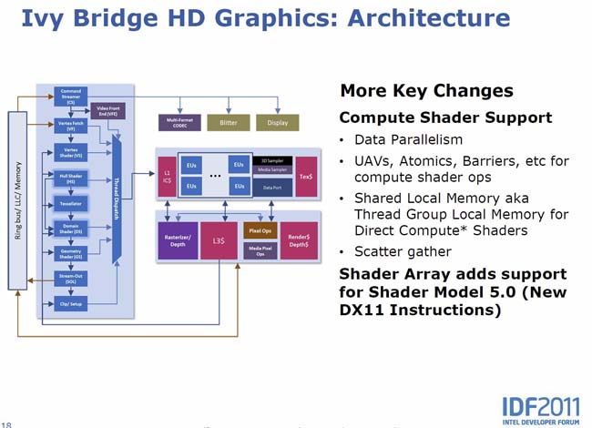
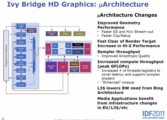
There are other microarchitectural changes on Ivy Bridge that makes it faster than Sandy Bridge. There is improved geometry performance, enhanced co-issue, and an increased number of threads/register. Ivy Bridge can co-issue twice as many FMA operations, and is able to perform twice as many MADs per clock vs the Sandy Bridge. If a particular task is not limited by the sampler or compute, we can expect to see double of performance.
According to Intel, the amount of scatter gathered per clock is 32x more than Sandy Bridge. From an actual performance standpoint, Intel states that there has been up to a 27x sustained performance gain in GPGPU workoad.
The Ivy Bridge GPU also adds support for three displays and faster Quick Sync encoding. The Sandy Bridge hardware decoder can decode 20x real-time HD data (ie. it can decode 20 concurrent streams or one stream at 20x the rate). For HD 1080p transcoding, it can achieve 5x the performance. With Ivy Bridge, thanks to microarchitectural changes such as enhanced performance for Multi-Format CODEC, increased Media Sampler Throughput, and performance scaling and other filters, we can expect the performance to be even better. In conjunction with the doubling of the media sampler and the additional EUs, the HD 4000 is able to encode at up to 2 times the speed of Sandy Bridge.
The power savings on Ivy Bridge also applies to the GPU. According to Intel, the GPU performance of Ivy Bridge would be double that of Sandy Bridge. In addition, we will see the same performance with half the power consumption. The 22nm fabrication, the improved instruction, extended co-issue, and the dedicated L3 cache help Intel to achieve this level of performance per watt.
The Ivy Bridge continues to enhance InTru 3D, Intel Insider 2.0 with Ultraviolet, and Intel Wireless Display technology. The Intel Insider is a security technology that is built into the processor designed to provide hardware-based protection to HD content online (a form of DRM). This feature first appeared on the Sandy Bridge processor, but now Intel has added support something called “Ultraviolet” that allows the 1080p content to be shared among multiple devices.
The Ivy Bridge Line-UP
Since the Ivy Bridge processors are the third generation Core processor, they will carry the model number 3000. As you may recall, the Sandy Bridge processors are the 2000 series. However, the Sandy Bridge E CPUs have also been labeled as part of the 3000 series so it can be slightly confusing. At launch, the fastest Ivy Bridge will have model number below 3800 while the Sandy Bridge E will have model numbers above 3800.
| Model | Base Freq/Max Turbo (GHz) | Cores/Thread | L3 Cache (MB) | Graphics | Base Freq/Max Dynamic (MHz) | TDP (W) | Price |
(USD)Core i7 3960X
(Sandy Bridge-E)3.3/3.96/1215N/AN/A130990Core i7 3930K
(Sandy Bridge-E)3.2/3.86/1212N/AN/A130555Core i7 3820
(Sandy Bridge-E)3.6/3.94/810N/AN/A130285Core i7 3770K 3.5/3.94/884000650/115077313Core i7 3770 3.4/3.94/884000650/115077278Core i5 3570K3.4/3.84/464000650/115077212Core i5 35503.3/3.74/464000650/115077194Core i5 34503.1/3.54/464000650/110077174Core i7 3770T2.5/3.74/884000650/115045278Core i7-3770S3.1/3.94/884000650/115065278Core i5 3550S3.0/3.74/462500650/115065194Core i5 3450S2.8/3.54/462500650/110065174Core i7 2700K
(Sandy Bridge)3.5/3.94/883000850/135095332Core i7 2600K
(Sandy Bridge)3.4/3.84/883000850/135095317Core i7 2600
(Sandy Bridge)3.4/3.84/882000850/110095294Core i5 2500K
(Sandy Bridge)3.3/3.74/463000850/110095216Core i5 2500
(Sandy Bridge)3.3/3.74/462000850/110095205
The top of the line Ivy Bridge is the Core i7-3770K running at a 3.5GHz core clock and a Turbo capability up to 3.9GHz. The CPU has a TDP of 77W and comes with 8MB L3 cache. This is a quad core processor with HyperThreading support. Comparing this to the Core i7 2700K, we can see that the clockspeed and the cache amount are actually the same on both CPUs.
Interestingly, the Core i7 3770K is priced at $313, cheaper than the Core i7 2600K and the Core i7 2700K that it is replacing. If we look at the rest of the line-up, we can see Intel prices Ivy Bridge $5-$10 cheaper than the Sandy Bridge lineup. Thus, if we consider the performance per dollar, the Ivy Bridge should be slightly better.
The Ivy Bridge will work on any Socket 1155 motherboards (both older 6 series and newer 7 series). However, to really take the full advantage of the features such as 3 display support and PCI-E 3.0, it is recommended to use the 7 series chipset. The older 6 series motherboards will need a BIOS update before they can recognize the processor. Since the socket is the same, there should be no issue with coolers either. We have done an extensive look at the features on the 7 series chipsets and board reviews. If you need decide whether to upgrade to a new motherboard, please check out our other article.
The Sandy Bridge has a greater differentiation between the Core i7 and Core i5 but with Ivy Bridge, the difference between Core i7 and Core i5 is merely the HyperThreading support and the amount of L3 cache. The i7 models all support HyperThreading and come with 8MB L3 cache while the i5 CPUs lack Hyperthreading support and come with 6MB of L3 cache. Other than these differences, all 77 Watt Ivy Bridge CPU’s come in quad core variants with HD 4000 GPU and the only difference between them is the clockspeed. Notice that the Core i5 3450 has a lower GPU dynamic clockspeed and some of the lower power CPU models (S models) come with HD 2500 graphics as opposed to HD 4000.
Overclocking
Current generations of processors are tightly integrated with the processor core (North Bridge) and sometimes the integrated graphics. As a result, traditional overclocking by raising the front side bus (FSB) to gain additional CPU clockspeed is much restricted since raising the FSB impacts not just the CPU clockspeed but also the PCI Express and the memory clockspeed. This limitation is not limited to the Intel processors, and also applies to AMD’s Bulldozer and Llano processors. Luckily, both Intel and AMD have processors with unlocked multipliers aimed at enthusiasts who wish to push gain that extra performance out of their chip.
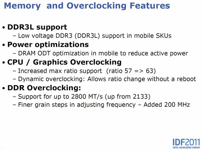
With the Sandy Bridge, Intel set the max ratio to 57, so that it is possible to overclock the Core i7 2600K to 5.7GHz (or slightly higher if you tinker with the BCLK). The Sandy Bridge BCLK often has about 5% leeway from its default speed of 100MHz, so with Sandy Bridge, the highest speed possible is about 6GHz (105MHz x 57). Intel raised the overclocking ceiling for the Ivy Bridge to 63 so the Ivy Bridge is easily able to break 6.0GHz by simply raising the multiplier. The Ivy Bridge has the potential of hitting 6.6GHz (105MHz x 63) and possibly even higher.
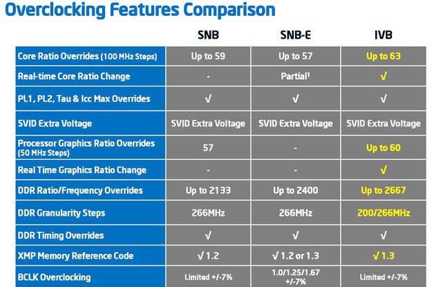
As mentioned earlier, the Ivy Bridge supports memory in increments of 200MHz and 266MHz and the maximum supported memory frequency is 2133MHz.The finer frequency stepping allows a greater control over the memory which should help with the stability.
Despite its overclocking potential, Ivy Bridge overclocking may not yield results better than (or even as good as) the Sandy Bridge on air cooling. Ivy Bridge overclocking is limited by the high heat output. Despite the die-shrink, the Ivy Bridge is packed with more transistors. The higher transistor density means there is just too much heat being generated for the heatsink to properly and effectively dissipate. It is possible that Intel still needs to perfect its tri-gate transistor technology to really effectively reduce the overall power consumption and heat output. The tri-gate transistor scales better at low voltage (below 1V), but as we crank up the voltage in order to overclock our chip, the power consumption and heat increase significantly.
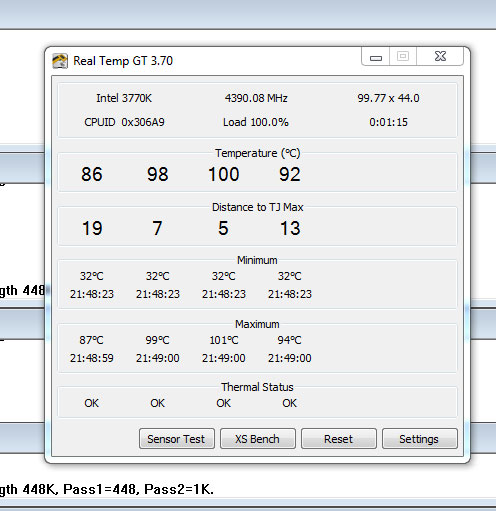
With the Intel motherboard, we were able to overclock the Core i7 3770K to 4.4GHz with the automatic setting that has been preset in the BIOS. (CPU voltage = 1.40V, Processor TDC Current Limit Override = 165 A). We also tested the processor in the MSI Z77A-GD65 and were able to overclock our processor to 4.7GHz without any issue. However, at this speed, the processor temperature reaches an alarming 100°C (98°Core) with our Zalman CNPS9900 MAX within a couple minutes of running Prime95. Not wanting to damage our sample, we did not run the usual 30 minutes Prime95 like what we usually do. At this speed, the system power consumption is 108W higher than the stock speed.
Overclockers probably will be very disappointed with the Ivy Bridge overclocking. Unless you plan to use liquid nitrogen, do not expect the Ivy Bridge to have the same level of overclocking as the Sandy Bridge.
Temperature

To test for temperatures, we ran Prime95’s Blend stress test for 30 minutes and we have recorded the results. Then we waited for another 30 minutes before we wrote down the idle temperatures.
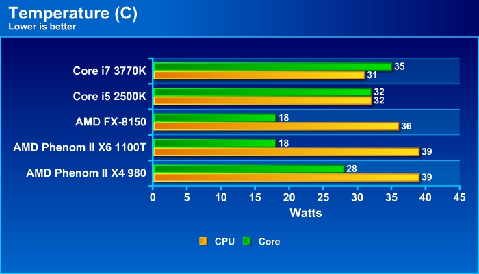
Coolers designed to work with the Sandy Bridge will work with the Ivy Bridge, but expect to higher temperatures. Idle, the Ivy Bridge CPU temperature for the Core i7 3770K is 1°C higher than the Core i5 2500K; however, the core temperature is 3°C higher.
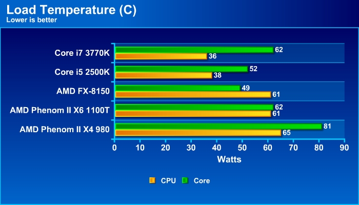
Under load, the Core i7 3770K is hotter. The CPU temperature is 5°C hotter and the Core is 10°C hotter. There is simply too much heat built up inside the CPU for the cooler to efficiently dissipate. The 10°C might not be an issue for a full or mid-tower system, but if you plan to put the processor inside a small form factor PC or mini-ITX system for an HTPC, it may not able to keep the chip cool enough. It also means the noise level may also be louder with the Ivy Bridge.
Power Consumption

For overall CPU power consumption, we have ran Prime 95’s Blend stress test. The highest number we saw on our wattage meter was recorded for maximum Watts used at by the CPU, while for idle we took the lowest wattage number after we shut down the application. Do remember that the wattages below do have additional hardware power consumption in it, including hard drives, SSDs, video cards, etc.
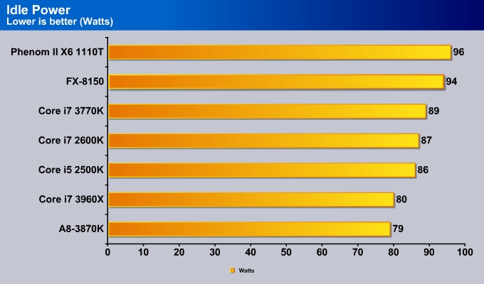
The Idle Power consumption for the Core i7 3770K is 2 watts higher than that of the Core i7 2600K. This is somewhat unexpected since the tri-gate transistor should help with lowering the power consumption. This is not a board issue as we noticed the same 1-2 watts difference with the MSI board.
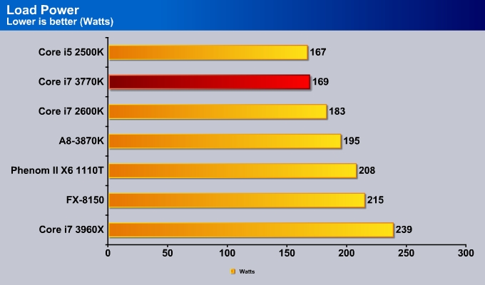
The load power is much better. The Core i7 3770K consumes 14 watts less power than the Core i7 2600K. Interestingly, the Core i5 2500K (which is also a 95W CPU without hyperthreading support) actually consumes a tad less power than the Core i7 3770K.
Testing & Methodology
In the interests of thoroughness and accurate results, we run each test at least three times, and some tests more than that. We average the total of all the tests from each benchmark then report the average here. If we had any ambiguous results we left those out and ran the benchmark once again.
The OS we use is Windows 7 Pro 64bit with all patches and updates applied. We also use the latest drivers available for the motherboard and any devices attached to the computer. We do not disable background tasks or tweak the OS or system in any way. We turn off drive indexing and daily defragging. We also turn off Prefetch and Superfetch. This is not an attempt to produce bigger benchmark numbers. Drive indexing and defragging can interfere with testing and produce confusing numbers. If a test were to be run while a drive was being indexed or defragged, and then the same test was later run when these processes were off, the two results would be contradictory and erroneous. As we cannot control when defragging and indexing occur precisely enough to guarantee that they won’t interfere with testing, we opt to disable the features entirely.
Prefetch tries to predict what users will load the next time they boot the machine by caching the relevant files and storing them for later use. We want to learn how the program runs without any of the files being cached, and we disable it so that each test run we do not have to clear pre-fetch to get accurate numbers. Lastly we disable Superfetch. Superfetch loads often-used programs into the memory. It is one of the reasons that Windows occupies so much memory. Vista fills the memory in an attempt to predict what users will load. Having one test run with files cached, and another test run with the files un-cached would result in inaccurate numbers. Again, since we can’t control its timings so precisely, it we turn it off. Because these four features can potentially interfere with benchmarking, and and are out of our control, we disable them. We do not disable anything else.
Test Rig
| Test Rig | |
| Case | Cooler Master Storm Trooper |
| CPUs | Intel Core i7 3770K (Ivy Bridge – LGA 1155 -Z77) |
Intel Core i7 3960X (Sandy Bridge-E – LGA2011 – X79)
Intel Core i7 2600K (Sandy Bridge – LGA1155 – Z77)
Intel Core i7 2500K (Sandy Bridge – LGA1155 – Z77)
Intel Core i7 980X (Gulftown – LGA1366 – X58)
AMD FX-8150 (Bulldozer – Socket AM3+)
AMD Phenom II X6 1100T
AMD Phenom II X4 980
AMD A8-3870KMotherboardsIntel DZ77GA-GD65
Intel DX79SI (Siler) X79 Chipset Motherboard
GIGABYTE GA-X58A-OC X58 Chipset Motherboard
ASUS Crosshair V Formula
Gigabyte A75M-UD2HRamKingston HyperX Gray 4 GB (2x2GB)CPU CoolerThermaltake SI-128 for AMD
Zalman CNPS9900 MaxHard DrivesSeagate Barracuda XT 3TBSSD1x OCZ Vertex 3 240GB SATA III 6Gb/s SSDOpticalASUS DVD-BurnerGPU1x Gigabyte GeForce GTX580 SOCPSUCooler Master Silent Pro Gold 1200W PSUMouseRazer Imperator Battlefield 3 EditionKeyboardRazer Blackwidow Ultimate Battlefield 3 Edition
Test Suite
We will use the following applications to test the performance of the Z77 Chipset (Motherboard, Processor).
| Benchmarks |
|---|
| PCMark 7 |
| 3DMark 11 |
| 3DMark Vantage |
| Cinebench R11.5 |
| SiSoft Sandra 2012b |
| X264HD |
| Truecrypt 7.1 |
| Unigine Heaven 2.5 |
| Metro 2033 |
| Lost Planet 2 |
| Alien vs Predator |
| Warhammar |
| Dirt 2 |
| Aida64 |
aida64 v2.3
“AIDA64 Extreme Edition is a streamlined Windows diagnostic and benchmarking software for home users. AIDA64 Extreme Edition provides a wide range of features to assist in overclocking, hardware error diagnosis, stress testing, and sensor monitoring. It has unique capabilities to assess the performance of the processor, system memory, and disk drives. AIDA64 is compatible with all current 32-bit and 64-bit Microsoft Windows operating systems, including Windows 7 and Windows Server 2008 R2.”
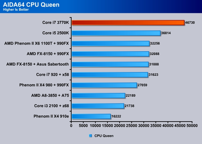
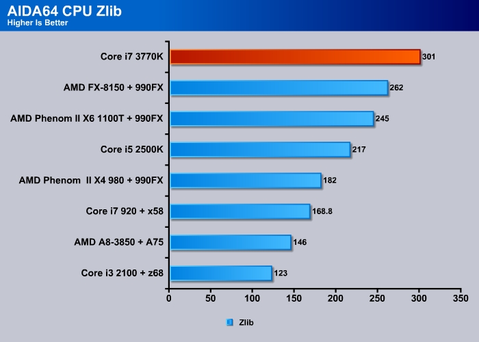
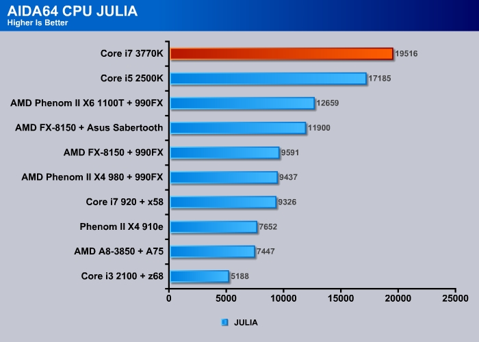
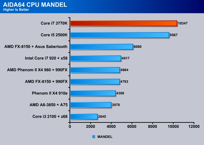
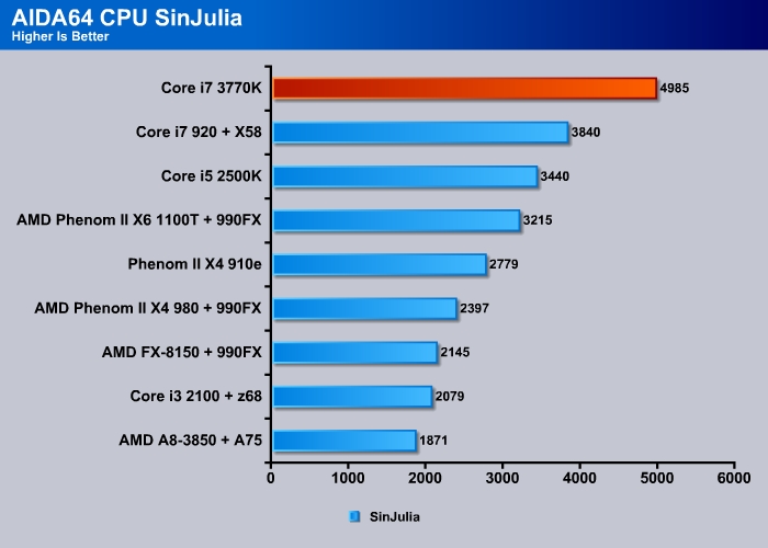
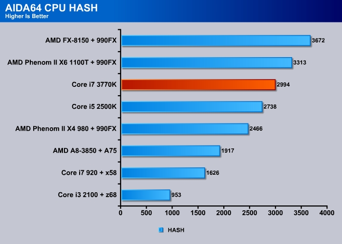
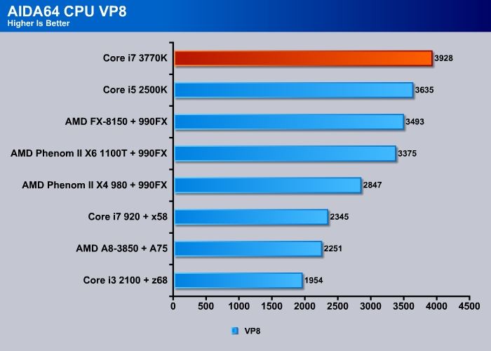
CPU
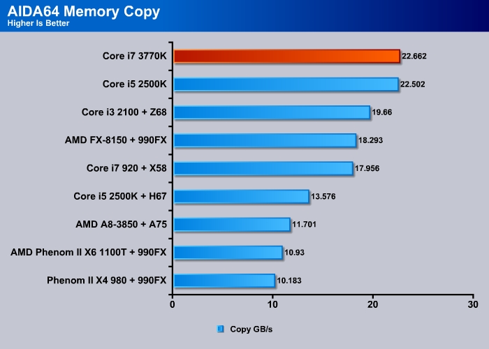
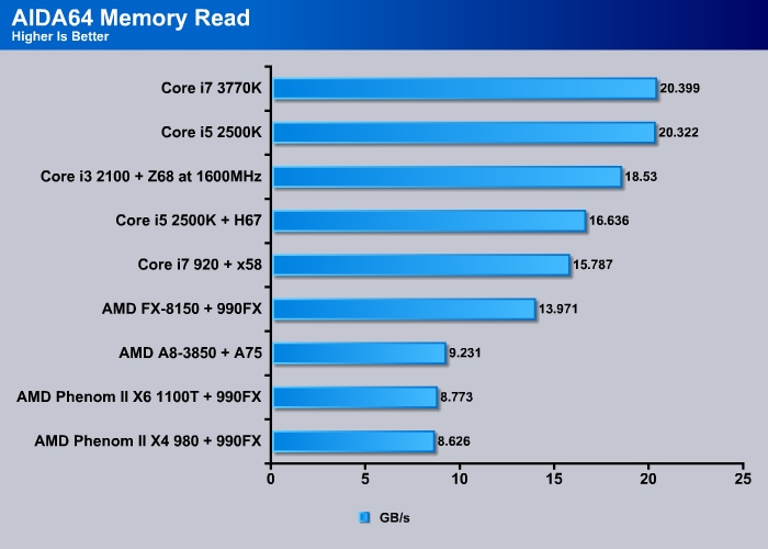
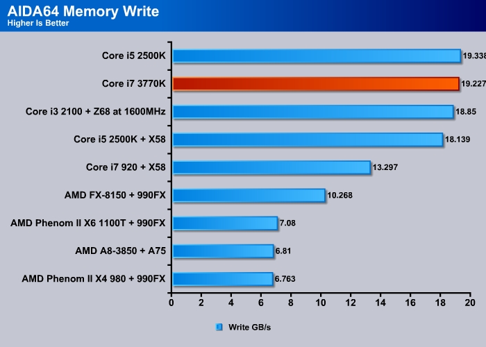
Memory
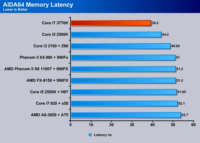
When comes to memory performance, the Ivy Bridge has improved slightly on the Copy and Read but the Sandy Bridge is a tad faster in the Write. The difference between the two is pretty slim; we think they are essentially identical. Intel has not really changed the memory controller on the Ivy Bridge as it is still a dual-channel at 1600MHz supported speed, so we do not expected to see as big of a difference. However, the Ivy Bridge shows a big improvement in terms of the Latency where we see 5ns faster over the Sandy Bridge. The shorter latency should make the Ivy Bridge performs tasks much quicker as long as it is not starving for the bandwidth.
Sisoft Sandra 2012b
“SiSoftware Sandra (the System Analyzer, Diagnostic and Reporting Assistant) is an information & diagnostic utility. It should provide most of the information (including undocumented) you need to know about your hardware, software and other devices whether hardware or software. It works along the lines of other Windows utilities, however it tries to go beyond them and show you more of what’s really going on. Giving the user the ability to draw comparisons at both a high and low-level. You can get information about the CPU, chipset, video adapter, ports, printers, sound card, memory, network, Windows internals, AGP, PCI, PCI-X, PCIe (PCI Express), database, USB, USB2, 1394/Firewire, etc.”
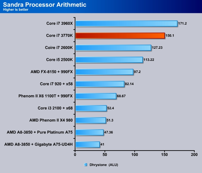
Sandra’s Dhrystone tests the processor’s integer performance and we can see the Ivy Bridge is 18% faster than the Sandy Bridge.
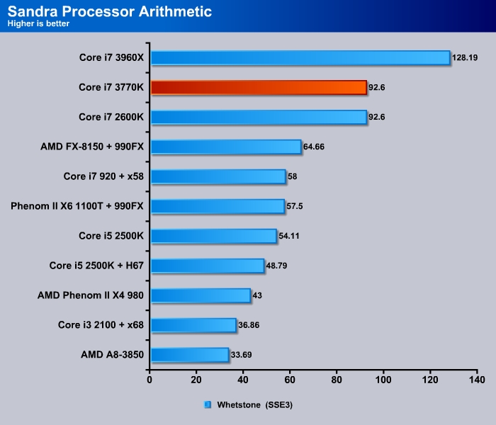
Whetstone tests the processor’s floating point calculation and we did not see any difference between the Core i7 3770K and the Core i7 2600K.
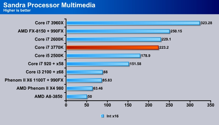
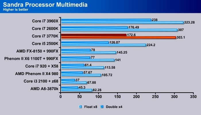
The Sandra Processor Multimedia test involves the generation of Mandelbrot Set fractals that are used to realistically describe and generate natural objects such as mountains or clouds. The Core i7 2600K performs just a tad faster than the Core i7 3770K. We are curious to see whether the difference is due to the new Power Aware Interrupt Routing (PAIR) that potentially directs the workload to the active core rather than the rest of the chip.
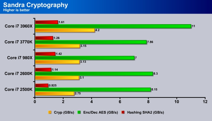
Sandra’s Cryptography benchmark is designed to measure AES encryption/decryption and SHA cryptographic performance. The Ivy Bridge is about 10% faster here.
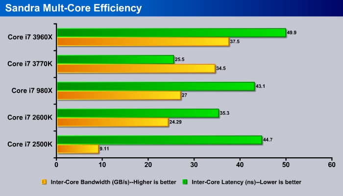
The multi-core bandwidth has been improved on the Ivy Bridge and we can see about 50% improvement here. What is even more impressive is the Inter-Core latency where the Ivy Bridge is able to improve it by 27%, making the interconnection between the processor cores even faster.
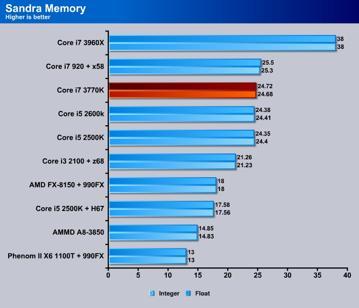
The memory bandwidth on the Ivy Bridge shows a small improvement over the Sandy Bridge but it is nothing dramatic. We probably would have to wait for the next architectural change to see a higher bandwidth.
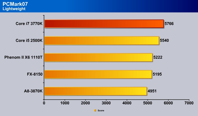
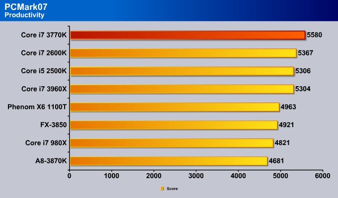
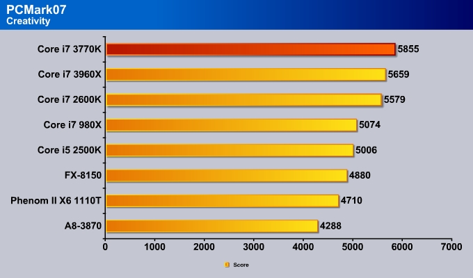
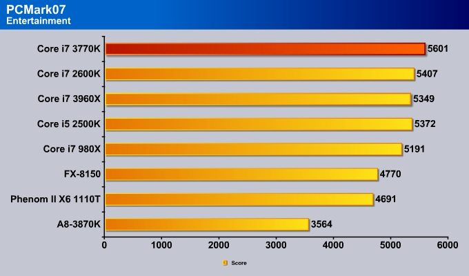
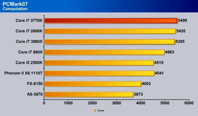
PCMARK 7
The latest benchmark Suite–PCMark 7, puts a greater stress on the system than the PCMark Vantage. Contrast to the PCMark Vantage, the latest edition stress type of workloads rather than individual tasks. It consists of Lightweight, Productivity, Productivity, Entertainment, Computation and Storage benchmark. Readers can refer to the PCMark 7 whitepaper for the detail list of applications and tests run for each suite.
PCMark 7 is not particularly heavy threaded and may not always stress the CPU’s full capability. However, it is nonetheless a good tool to get a sense of how a CPU performs in day to day tasks.
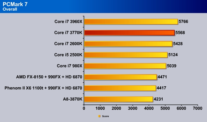
Overall, the Core i7 3770K performs quite well. It scored 2.5% in the overall score over the Core i7 2600K.
When we look at the individual tests, we can see that the Core i7 pretty much takes the lead with 3~5% gain over the Core i7 2600K. This is within what Intel expects the processor to perform. There is no major architectural change with the Ivy Bridge, so there is no major CPU performance difference between it and Sandy Bridge.
Cinebench and R11.5
“CINEBENCH is a real-world test suite that assesses your computer’s performance capabilities. MAXON CINEBENCH is based on MAXON’s award-winning animation software, CINEMA 4D, which is used extensively by studios and production houses worldwide for 3D content creation. MAXON software has been used in blockbuster movies such as Spider-Man, Star Wars, The Chronicles of Narnia and many more. MAXON CINEBENCH runs several tests on your computer to measure the performance of the main processor and the graphics card under real world circumstances. The benchmark application makes use of up to 16 CPUs or CPU cores and is available for Windows (32-bit and 64-Bit) and Macintosh (PPC and Intel-based). The resulting values among different operating systems are 100% comparable and therefore very useful with regard to purchasing decision-making. It can also be used as a marketing tool for hardware vendors or simply to compare hardware among colleagues or friends.”
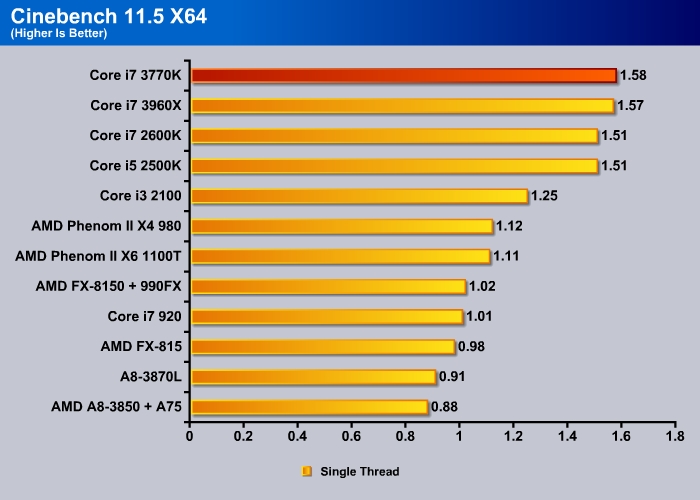
Since Ivy Bridge is able to Turbo to 3.9GHz with only a single thread, it performs just like the Core i7 3960X. In fact, it scored 0.01 points higher. The Turbo feature with the Ivy Bridge seems to be much faster then the Ivy Bridge and as result, it may help out with the slightly performance enhancement.
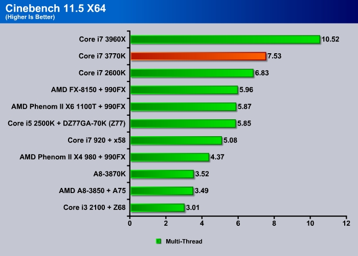
The multi-thread performance on the Core i7 3770K is about 10% faster than the Core i7 2600K.
Truecrypt 7.1

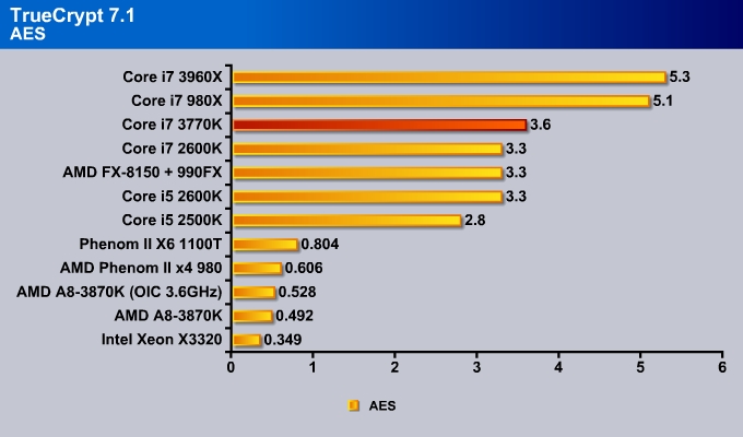
When comes to data encryption, the Core i7 3770K is about 9% faster than the Core i7 2600K. The improvements on the float-point calculation of the Ivy Bridge most likely contributed to the performance gain. Notice that this puts the Core i7 3770K faster than the AMD FX-8150.
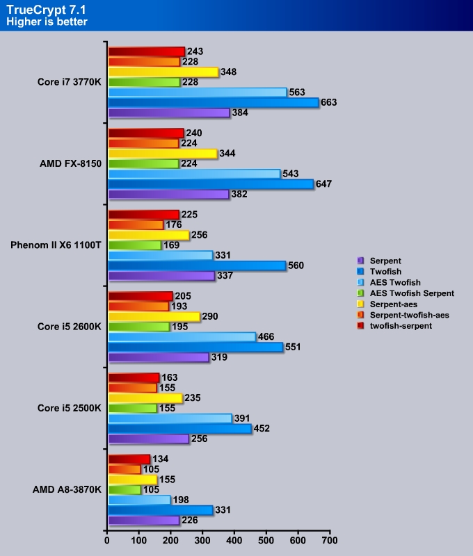
More detailed comparison of other data encryption methods from TruCrypt. Again, notice that the Core i7 3770K edges out the FX-8150 in every single test. Data encryption is one area where AMD Bulldozer has a slight advantage but the Core i7 3770K has put the Intel back to the top.
X264HD

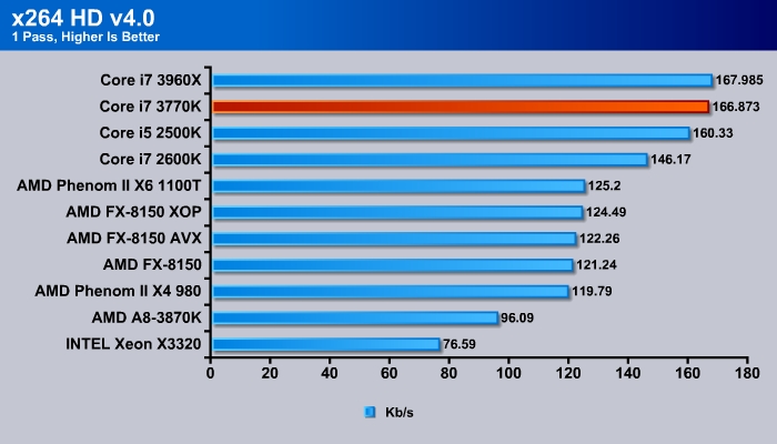
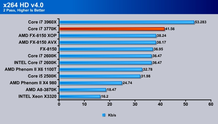
When comes to media transcoding, the Core i7 3770K falls just behind the six-core Core i7 3960X. This is also an area where the AMD FX-8150 had a slight edge over the Sandy Bridge, but once again the Core i7 3770K with a 15% improvement over the Core i7 2600K jumped ahead of the FX-8150.
Media Expresso 7: QuickSync in Action
![]()
Intel has made some improvements with the QuickSync where the media transcoder is capable of doing twice of MAD calculation. As a result, we see that the transcoding performance of the HD 4000 is double of what we have seen on the HD 3000. Keep in mind that the performance gain only applies to the HD 4000 and not to the HD 2500. Since the HD 2500 still only has one media transcoder, it should perform approximately equal to the HD 3000.
3DMark Vantage
![]()
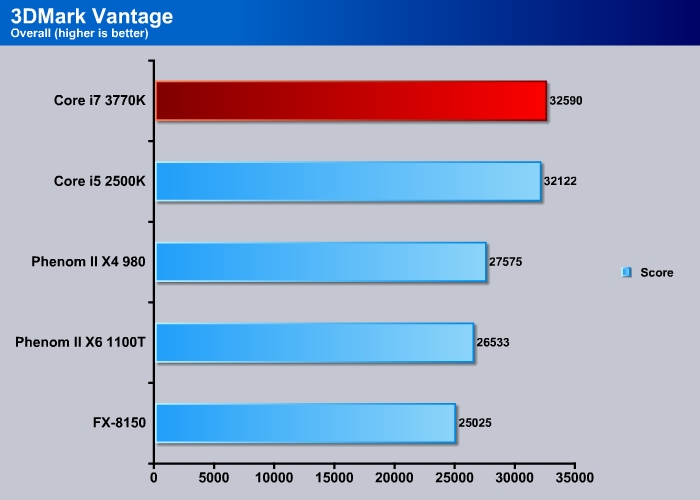
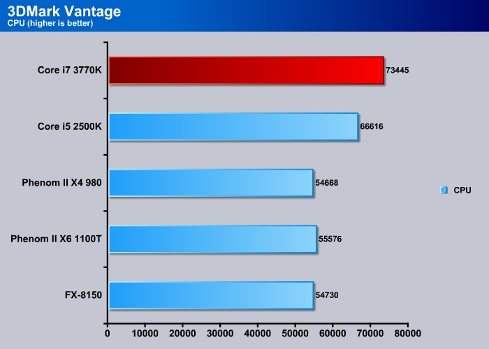
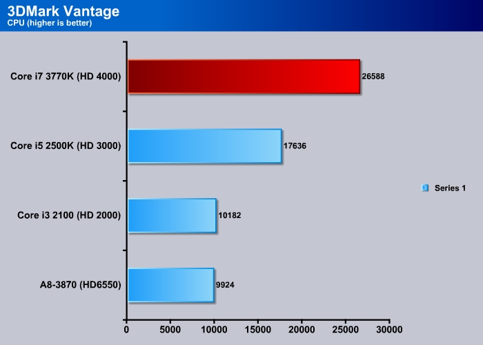
There is about a 1% difference in the 3DMark Vantage overall score between the Core i7 3770K and the Core i5 2500K. When we look at the CPU score, we can see the Core i7 3770K is about 10% faster.
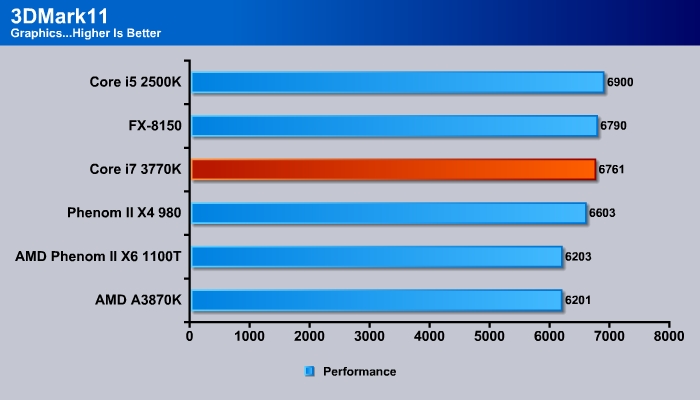
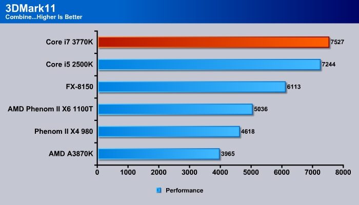
3DMark 11
![]()
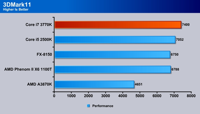
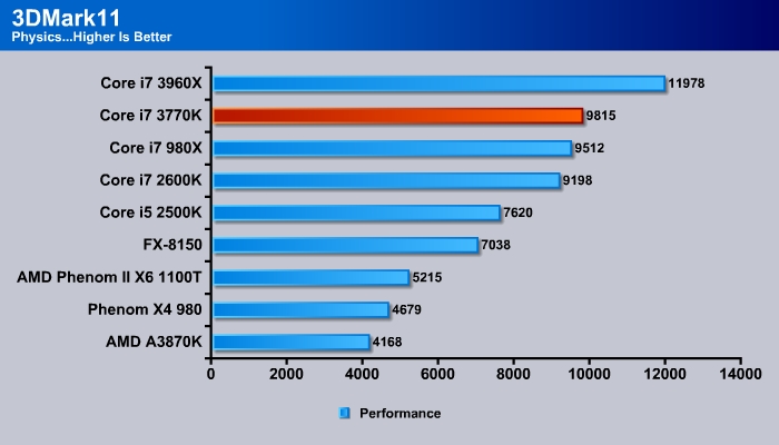
3DMark11 Physics tests the processor’s performance. Here we can see the Core i7 3770K is 3% faster than the Core i7 2600K.
Performance with GTX 580
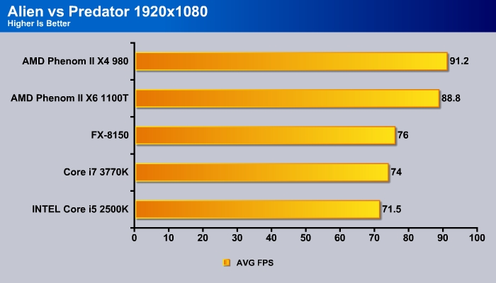
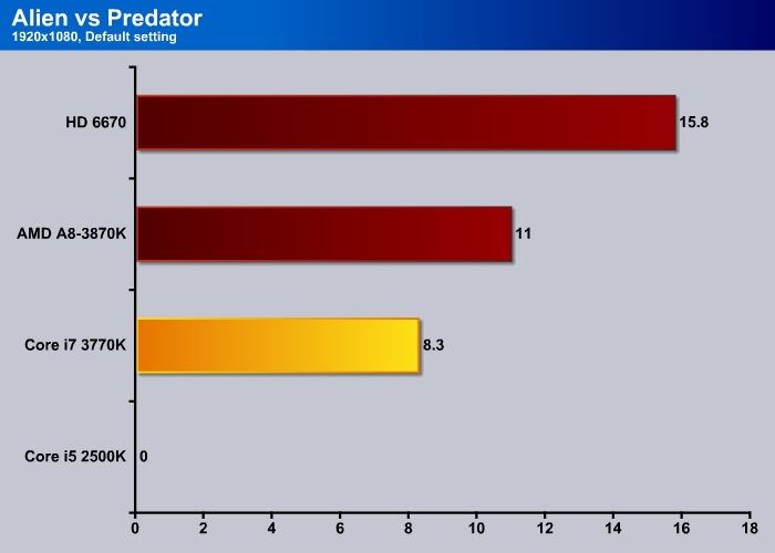
We start off with the Alien vs Predator to give you some idea that not all of the games stress the processor that much, and as you can see the AMD processors seemed to perform better here. The Core i7 3770K does manage to gain a couple of points over the Core i5 2500K.
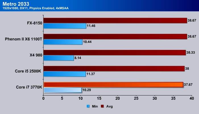
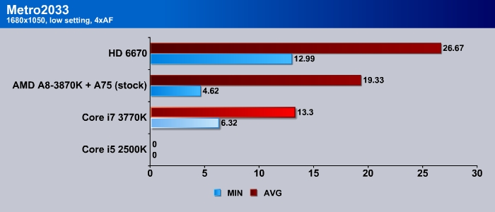
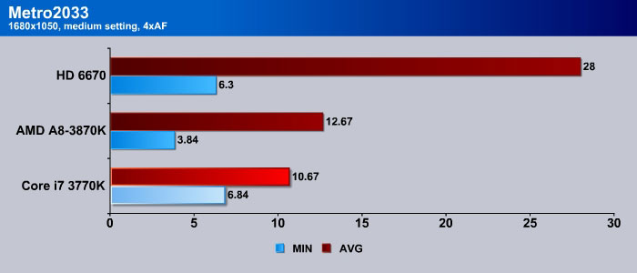
Turning to Metro 2033 we can see that the CPU’s impact on the gaming performance is not as big either, even at 1920×1080.
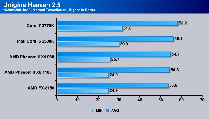
With Unigine Heaven 2.5, we can see that the Core i7 377K is about 5% faster than the Core i5 2500K.
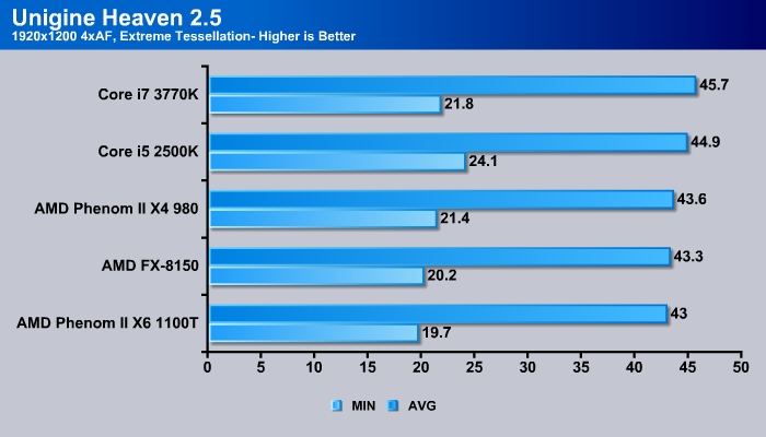
As we turn the Tessellation up to Extreme, the Core i7 3700K still manages to to edge out the Core i5 2500K by a 2% average framerate but the Core i5 2500K actually scored better in the minimal frame.
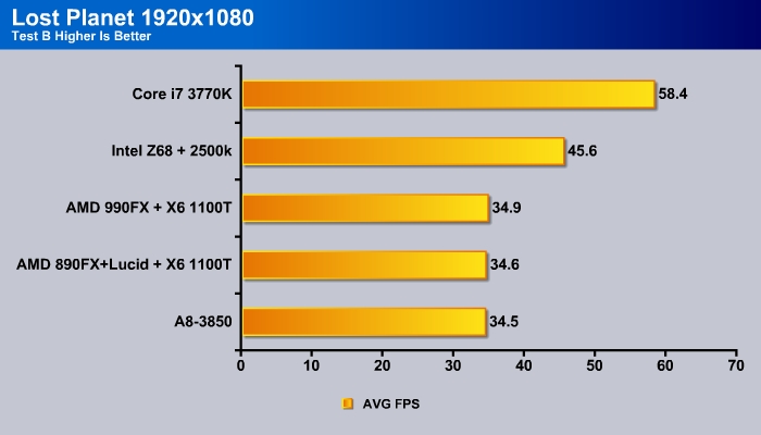
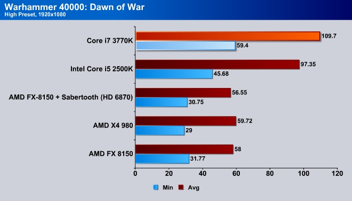
Lost Planet 2 and Warhammer 4000: Dawn of War both scale better with the CPU. Here we see that the Core i7 3770K is 28% and 13% faster than the Core i5 2500K in Lost Planet 2 and Warhammer, respectively.
HD 4000: A step further
3DMark Vantage
Let’s start by comparing the HD 4000 to the HD 3000. We can see that the new GPU is about 70% faster than the HD 3000 when we look at the overall score from 3DMark Vantage. Despite the improvement, the AMD HD 6550D is still even faster.
Bear in mind that we use the Core i5 2500K which also has the HD 3000 like the Core i7 2600K, except that it runs at 1000MHz as opposed to 1350MHz.
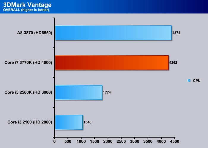
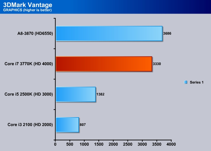
When we look at the GPU score, we see the HD 4000 actually yields more than double of the performance over the HD 3000 (150%). We include the Core i3 2100 with HD 2000 to give our readers an idea what to expect with the HD 2500. Intel claims that the HD 2500 would be about ~20% faster than the HD 2000, so we can see that even with the improvement, the HD 2500 is still going to be slower than the HD 3000.
AMD is still having a bit of an edge with the integrated graphics, and we can see that the the HD 4000 is still not up to the level of the HD 6550 on the AMD A8-3870K.
While falling behind in the GPU, Intel is clearly dominating the CPU front.
3DMark 11
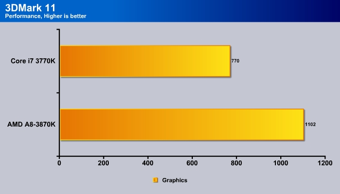
The 3DMark 11 is a DirectX 11 test that puts a greater demand on the graphics. We can see the HD 4000 is still lagging behind the HD 6550D on the AMD A8-3870K. The AMD integrated GPU is still about 40% faster than the Intel. AMD is planning to release Trinity (the successor to Llano), which should widen the separation even further.
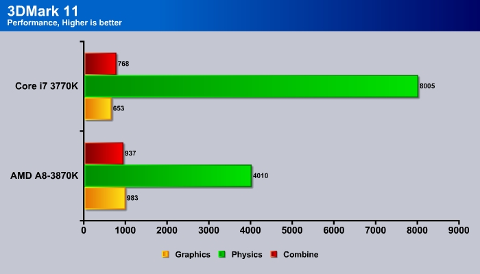
If we look at the individual tests, we can see the that the A8-3870K is about 50% faster in GPU but the Intel is about twice as fast in the CPU department (physics calculations).
HD 4000 (Core i7 3770K) vs HD 6550D (A8-3870K)
Let’s see how the integrated graphics fare in actual games.
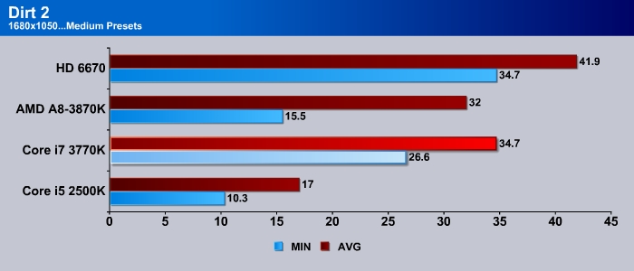
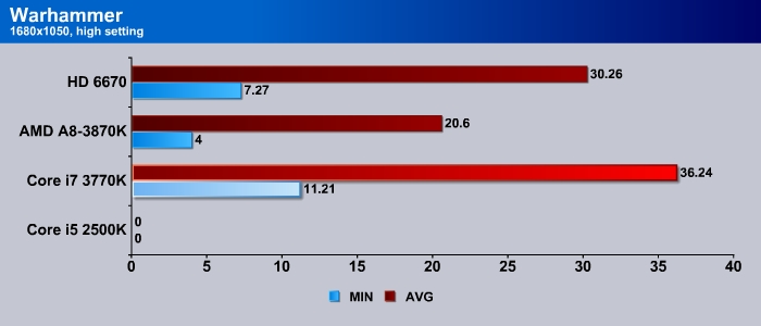
With the exception of Dirt 2 and the Warhammer (which are more CPU bound than GPU bound), the HD 4000 on the Core i7 3770K still falls the HD 6650D. Depending on the games, we see it is about 20% to 200% 30% slower .
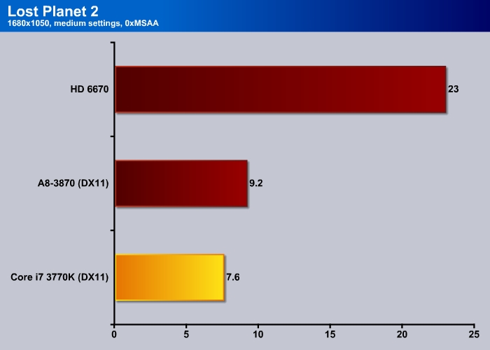
Note, we originally made a mistake entering the Lost Planet 2 result for the AMD A8-3870, the chart above shows the correct result where the Intel GPU is about 17% slower than the AMD GPU.
The HD 4000 is a great improvement from Intel with its doubling of the performance over the previous generation and we are glad to finally see it includes the support for DirectX 11 and OpenCL. The HD 4000 is definitely a welcome development. While it may not be as fast as AMD’s offering, we are glad to see Intel is serious at offering competitive graphics on their CPU. With the HD 4000, we noticed that games load faster and it appears to be running much smooth than the HD 3000 even when it is still not up to what AMD is offering.
At this moment, AMD is still competitive on the GPU front as Llano is still a nice chip with decent CPU power and a better GPU. However, if Intel continues with the same pace of improvements, then AMD would have a major concern.
GPU Compute Power
Let’s take a look the theoretical GPU compute power of the HD 4000. We ran Sandra’s GP Computing benchmarks. Keep in mind that these numbers are theoretical performance.
The HD 4000 finally added support for OpenCL v1.1 and OpenGL 3.1 on both the CPU and GPU. Previously, the Sandy Bridge only supported OpenCL on the CPU, and the GPU could run DirectCompute shader. Now we can finally tap into the Ivy Bridge’s execution units for compute power.
GP Processing
OpenCl GP Processor
| OpenCl GP | Native Float Shader (Gbpix/s) | Native Double Shader (Mpix/s) |
| Core i7 2500K (HD 3000) | 0.10388 | 43.3 |
| Core i7 3770K (HD 4000) | 0.15791 | 72.75 |
| GTX 580 | 1.86 | 304.23 |
| % increase over HD 3000 | 52% | 60% |
The HD 4000 OpenCl compute is 52% faster in the float shader and 60% faster in the double shader than the HD 3000
| Compute Shader | Native Float Shader (Gbpix/s) | Native Double Shader (Mpix/s) |
| Core i7 2500K (HD 3000) | 0.05881 | 5 |
| Core i7 3770K (HD 4000) | 0.27276 | 57.2 |
| GTX 580 | 1.86 | 304.23 |
| % increase over HD 3000 | 363% | 912% |
We see a huge gain in the Ivy Bridge’s GPU compute power. Part of the reason maybe the dedicated L3 cache on the GPU.
GP Cryptography
| Compute Shader | Cryptography Bandwidth (GB/s) | Encryption/Decryption Bandwidth (GB/s) | Hashing Bandwidth (GB/s) |
| Core i7 2500K (HD 3000) | 0.363 | 0.129 | 1.019 |
| Core i7 3770K (HD 4000) | 1 | 0.902 | 1.15 |
| % increase over HD 3000 | 175% | 599% | 12.9% |
In the Cryptography benchmark, we can see there is a huge gain in the encryption/decryption bandwidth most likely due to once again the L3 cache. The Hashing bandwidth shows a small 12% gain.
GP Bandwidth
| Compute Shader | Internal (GB/s) | Transfer (GB/s) |
| Core i7 2500K (HD 3000) | 8 | 3.29 |
| Core i7 3770K (HD 4000) | 14.77 | 6.7 |
| % increase over HD 3000 | 84.6% | 103% |
The bandwidth on the HD 4000 is twice as fast as the HD 3000.
conclusion
Intel tried to do more with the Ivy Bridge than what they used to do with a standard “tick”. The combination of the 22nm die-shrink, the revamped GPU architecture, and the use of tri-gate 3D transistors might have been too much to do in one step. As a result, Ivy Bridge is not perfect. As always with a major technological advance, there may be some setbacks. What looks good on paper may not always turn to be perfect in real-world.
Ivy Bridge certainly delivers many good things, including a much better GPU with DX11 support, higher CPU performance, lower overall system load power consumption, and even faster QuickSync. The only area where it falters is the heat output, which ultimately affects its overclockability. Taking everything into account, Ivy Bridge certainly moves Intel forward.
We can see that Intel is serious with their integrated graphics. Intel’s strongest competition from AMD is not in the CPU area, but in the integrated GPU. On the CPU front, Intel is untouchable and it will remain the top dog for the foreseeable future. But computing is shifting towards mobile and more portable and compact systems where integrated GPU’s are often being used. While the Ivy Bridge GPU is still not able to play most current titles at 1680×1050, it may be enough to handle games at 1366×768, the resolution of many laptops on the market. With Windows 8’s touchscreen-friendly Metro UI, we may finally see laptops move to a higher resolution like what we saw on smartphones and tablets, which would certainly need a much faster GPU to handle the higher resolution.
Ivy Bridge’s GPU moves Intel in the right direction. It is quite a task for Intel to deliver twice the performance of Sandy Bridge in 18 months, a pace that is even faster than many dedicated GPU manufacturers have managed, though Sandy Bridge did not set the bar too high. Still, if Intel continues at this pace, then the next generation of processor (Haswell) could finally bring us a strong GPU.
On the CPU front, Ivy Bridge is certainly delivers a respectable performance gain. The CPU is about 5-10% faster depending on the workload. The Sandy Bridge is already quite fast and it is difficult to improve the instruction per clock without a major architecture redesign. The improvements on the inter-core bandwidth and the latency will make the processor finish the task faster.
If you do a lot of video transcoding, Ivy Bridge will certainly make you more productive as we can see the transcoding time has been halved. The Sandy Bridge QuickSync was already impressive but the Ivy Bridge is even better. Be warned though, to really gain the double of the performance, you need to choose a CPU with HD 4000 and not HD 2500.
Obviously, the biggest issue with the Ivy Bride is its high heat output and the operating temperature. The chip certainly delivers lower power consumption under load (~20 watts less) but it also runs hotter. For desktops, the additional heat may not be an issue but for mobile users, the stronger cooling required due to higher heat output might cancel out any power saving. For desktop users, the higher operating temperature is not a major problem as long as you have proper cooling but it maybe less desirable if you are seeking for an absolutely quiet system. Of course, overclockers will be disappointed by this. While the platform has a great overclocking potential, it is ultimately being held back by its heat output.
Ultimately, if you already have a Sandy Bridge processor, there is no reason to upgrade to Ivy Bridge unless you only plan to use the integrated GPU and need the extra performance offered by the QuickSync. For those who are still using an older socket processor (Socket LGA775, LGA1156, or LGA1366), the Ivy Bridge upgrade is definitely a big step forward in both the power consumption and performance.