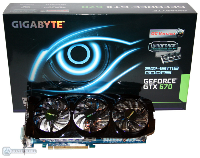
The GIGABYTE GTX 670 OC is a veritable force to be reckoned with not only for price versus performance, but in quality thermal design. Read on to find out!
Introduction
With the advent of the Kepler architecture there has been a rather wide price gap in dollar-versus-performance on the market. Hot on the heels of the GTX 680, GIGABYTE used NVIDIA’s GTX 670 reference design and boosted it with not only a factory overclock, but gave it a complete redesign in thermal and power management. The GIGABYTE GTX 670 OC sells for approximately $415. Let’s see how the latest competes with the other high-rolling single-core GPU’s on the market.
Clarifying the main differences in the GIGABYTE’s OC version of the GTX 670, there is a modest 10% factory overclock across the board. Noticeable differences right away are the cooling solution and slightly higher power requirements. Even though it shares more common characteristics of its older sibling, the GTX 680, one of the SMX processors is still disabled like the reference GTX 670. Below is the chart where GIGABYTE’s video card is highlighted in gold, while NVIDIA’s reference board line-up is highlighted in black.
| Specifications | GTX 680 | GIGABYTE GTX 670 OC | GTX 670 | GTX 580 |
|
CUDA Cores
(Stream Processors)
|
1536(GK104) | 1344(GK104) | 1344(GK104) | 512(GF110) |
| SMX | 8 | 7 | 7 | 16 |
|
Texture Units
|
128 | 112 | 112 | 64 |
|
ROPs
|
32 | 32 | 32 | 48 |
|
Base Clock
|
1006 MHz | 980 MHz | 915 MHz | 772 MHz |
|
Shader Clock
|
N/A | N/A | 950 MHz | 1544 MHz |
|
Boost Clock
|
1058 MHz | 1200 MHz | 980 MHz | N/A |
|
Memory Clock
|
6008 MHz GDDR5 | 6008 MHz GDDR5 | 6008 MHz GDDR5 | 4008 MHz GDDR5 |
| L2 Cache Size | 512KB | 512KB | 512KB | 768KB |
|
Memory Bus Width
|
256-bit | 256-bit | 256-bit | 384-bit |
| Memory Bandwidth | 192.2GB/s | 192.3GB/s | 192.2GB/s | 192.4GB/s |
| Texture Filter Rate | 128.8 GigaTexels/s | 109.8 GigaTexels/s | 102.5 GigaTexels/s | 49.4 GigaTexels/s |
|
VRAM
|
2GB | 2GB | 2GB | 1.5GB |
|
TDP
|
195W | 180W | 170W | 244W |
| Recommended Power | 550W | 550W | 500W | 700W |
| Power Connectors | 2×6-Pin | 1×6-Pin, 1×8-Pin | 2×6-Pin | 1×6-Pin, 1×8-Pin |
|
Transistor Count
|
3.5B | 3.5B | 3.5B | 3B |
|
Manufacturing
|
TSMC 28nm | TSMC 28nm | TSMC 28nm | TSMC 40nm |
| Thermal Threshold | 98C | 98C | 98C | 97C |
|
Launch Price
|
$499 | $415 | $399 | $499 |
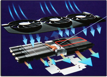
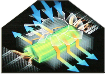
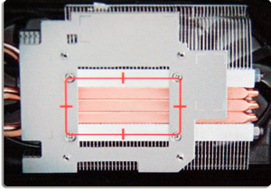
The benefits and differences between the Kepler and Fermi architectures has already been well covered and if so inclined, details can be found here. For now the focus is what differentiates the GIGABYTE GTX 670 OC and NVIDIA’s GTX 670 reference card. A three-step approach encompasses GIGABYTE’s patented cooling technology called Windforce 3X. Components such as the fans, heatsink block, and direct heat pipe touch technology are explored in finer detail below:
 |
Three ultra-quite PWM fans provide excellent air flow even when the card is under full load. The unique design combines the fins with a clip module providing an anti-turbulent shroud- housing. On the bottom is a special RAM heatsink optimized for heat transfer. | |
 |
The triangle design of the heatsink block further minimizes the flow of air turbulence between the fans and also provides the system with efficient air flow. | |
 |
Three 8mm pure copper heat pipes make direct contact with the GPU through direct heat pipe touch technology. A solder free process increases heat dissipation drastically. | |
You can also find our reference design NVIDIA GTX 670 review here to have a direct comparison with the GIGABYTE GeForce GTX 670 OC 2GB video card.
 Bjorn3D.com Bjorn3d.com – Satisfying Your Daily Tech Cravings Since 1996


I don’t notice the fan being to loud with in an inclosed case til around 65%, but the cooler is so good mine rarely ever gets to 50%. Hottest my card gets i 70-75c and that is with +60mhz OC so 1260mhz with boost and ram is overclocked from 6ghz to 7.2ghz.