Introduction
Today, NVIDIA is announcing it’s latest product, the second generation nForce motherboard chipset to support AMD’s Athlon family of Socket-A processors. As we discussed in our review of the original nForce platform, back in December 2001, nForce is a departure from traditional model the all-in-one motherboard solutions. They’ve incorporated audio, video, network, and high speed bus technology that make it stand above the eMachine class all-in-one motherboards. With this preview, we’ll review what NVIDIA has on the nForce platform and what’s new with nForce 2. We do not yet have a sample to test, so this preview is based upon press information provided by NVIDIA and on discussion with the NVIDIA staff.
Recap of the nForce Technology
The primary barrier of the existing motherboard architecture on the market has been the over reliance on the CPU for video based geometry calculations, the governing of applications, and the oversight of the peripherals attached to the Southbridge. NVIDIA, last winter, released heir first integrated motherboard chipsets entitled nForce.
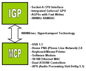 |
The nForce chipsets entitled Media and Communications Processor (MCP) and Integrated Graphics Processor(IGP) are a departure form the standard Northbridge and Southbridge configurations. NVIDIA, taking advantage of the wealth of technology and small die size construction available, has integrated state of the art audio, video, and networking components on the chipsets. In addition to the inclusion of these items, NVIDIA has bought off on the AMD consortium Hypertransport Technology. This technology, in nForce1, creates a data bus capable of up to 800MB/s between the Northbridge (IGP) and Southbridge (MCP). All of these features are shown on the diagram, at left, which helps identify where NVIDIA has empowered these new chipsets. |
Taking the burden away from the CPU of common and necessary tasks (audio encoding, network translation, etc. which can all be performed concurrently in parallel by hardware) frees up CPU clock cycles to perform other calculations of specific applications or other demands from hardware. This is a profound step in the direction of improving overall system performance. As an example, Scott had noted a minimal CPU load from the integrated 10/100 MAC on his nForce1 board of around 5% vs. a common 25-30% load of PCI network adapters.
To further detail what NVIDIA has included on these chipsets, the following table describes in detail what technology has been integrated:
| Technology | MCP | IGP | Description |
| Hyper-Transport | X | X | This is AMD’s high speed interconnection bus interface which controls traffic between the IGP and MCP at 800MB/s (roughly 6 times faster than the PCI bus). |
| StreamThru | X | – | Isochronous aware algorithms that are intended to provide clear and consistent throughput for video, audio, and other communications streams. These algorithms will all but eliminate CPU dependency for network and broadband data streaming. |
| Complete Communications Suite | X | – | HomePNA v.2.0 (Home Phone-line Network Adapter), USB, Software modem, 10/100 Ethernet MAC. |
| Dolby Digital 5.1 real-time encoder | X | – | NVIDIA’s APU (Audio Processing Unit) was an industry first, on-board real-time Dolby Digital 5.1 Encoder. The APU supports 2/4/6 channel outputs, DirectX8 3D audio in hardware (32 Hardware Submixers), 256 2D voices, 64 3D voices, and 3D positional audio. |
| TwinBank Memory Architecture | – | X | Unlike industry standard Shared Memory Architecture, a 128-bit wide 266MHz DDR memory path is maintained for the onboard graphics controller, resulting in 4.2GB/s peak memory bandwidth with minimum system latency. This low latency path is maintained by the use of crossbar technology that incorporates dual-independent, 64-bit memory controllers and a single master arbiter. |
| Dynamic Adaptive Speculative Pre-processor(DASP) | – | X | An innovative set of algorithms to reduce CPU system and memory access latency by monitoring CPU access patterns and developing call predictions such that needed data can be pre-staged for lower latency access. |
| Geforce2 GPU | – | X | Last, but not least, a Geforce2 GPU is embedded on the IGP chipset, offering the highest level of 3D graphics performance of any on-die chipset. |
To support this platform, NVIDIA has a Unified Driver and BIOS Architecture that is comprised of a single driver for graphics, IDE, and the complete communications suite. Additionally, the single driver also supports ALL of the current NVIDIA GPUs which will be automatically detected when installed in the AGP slot.
nForce2
So what’s new? The changes come primarily in the form of two new chipsets with some updates to the existing IGP and MCP chipsets. The System Platform Processor (SPP) and a revised model of the MCP, called MCP-T. All these chipsets might seem confusing. To best present these new chips and how they work with the original MCP and IGP, I’d first like to start with describing the technology on the new chips then describe how they integrate, since the technology may let you realize how they do integrate.
 |
|
 |
|
And, as I mentioned, the Integrated Graphics Processor from nForce1 has also been updated:
 |
|
 |
|
So, we have two new chipsets, and two existing nForce1 chipsets which have been updated with the latest tech. What do all these options mean to the user? What we have is basically FOUR pairs of chipsets available to motherboard manufacturers to form the North and Southbridges of a nForce2 motherboard. As the following diagram suggests, The SPP can take the place of the existing IGP chipset. In place of the MCP, the designer may choose to utilize the MCP-T, in order to capitalize on the advanced audio engine and the second and name branded (3COM) ethernet support.
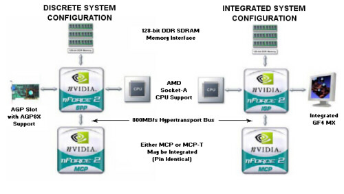
What we end up with is several choices for motherboard layout. The Discrete system, based on the SPP chipset with advanced DDR support and the lack of on-die video, will be the choice of the performance user who plans to rely upon state-of-the-art video adapters. While system built around the revised IGP chipset will prove to be a quality all-in-one solution for the budget user. NVIDIA showcased this market table in their press information on the nForce2:
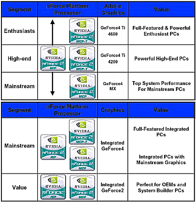
The top three options include the SPP chipset. Based upon the market data provided, it appears that ‘high end’ platforms (if you want the high-end audio, and maybe the second ethernet adapter) with be based upon the SPP and MCP-T combinations. There is also an option for the SPP coupled with the standard MCP chipset. I’d anticipate that this model might see the most production as the added ethernet adapter will see less use by gamers, IMO. The budget market with the IGP chipset, atleast includes a suggested MCP-T option. IMO, a quality integrated motherboard would be very appropriate for the SOHO server market, where the added ethernet adapter will see some use. Note that bottom rung of the ladder appears to be based upon the existing nForce1 IGP chipset with the integrated Geforce2. I’m uncertain if NVIDIA is still having the original IGP produced or if there is still a significant number of these chips in the market. I’m also unsure of whether or not this market segment suggests the use of the old MCP or newly revised MCP. It would be nice if the new MCP is at least used here for the USB2, Firewire, and ATA133 support. It’s also important to note that NVIDIA’s table for the SPP and IGP platforms varies mainly by the suggested video adapter.
Performance
Since we don’t yet have our greasy mitts on an nForce2 to test, we must rely upon the information provided by NVIDIA. The NVIDIA press info contained two graphs of benchmarks of the new IGP with the integrated Geforce4 MX GPU. One of 3DMark2001 and Quake 3 Arena benchmarks of several different platforms (all with integrated video). The graphs also compare the older nForce1 chipsets, the 420 and 220.
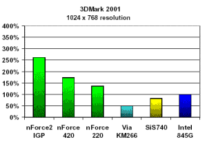
3DMark2001 is a DirectX8 engine. Since the integrated Geforce4 MX is not a DirectX8 part (lacking the pixel and vertex shaders included in the Geforce3s, Geforce4 Tis, and Radeons) it must rely upon its standard rendering pipeline and speed of the memory available to it over the integrated bus. Perhaps not so surprising, the new IGP surpasses the older nForce 420 chipset by a good 55-60%.
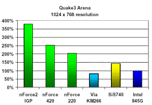
Again, the integrated Geforce4 MX surpasses the nForce 420 by a decent margin. This time it’s not quite as far as the 3DMark scores for this OpenGL engine. This time, though, it’s still by a healthy 45%. Any way you look at it, it’s heads and above what anyone else is currently offering for integrated video. Relative performance can be misleading, however. We’ll have to hold our verdict until an nForce2 makes it’s way into the Bjorn3D labs.
Conclusions
On one hand it appears NVIDIA is only offering an updated nForce platform that is merely staying on top of the technology wave by including USB2 support, Firewire support, ATA133 support, etc. But, on the other hand, we have some innovative technology also. DualNet ethernet adapters; on-board Geforce4 MX power with promised dual display support; integrated Internet Connection Sharing and Internet Connection Firewall support; and DDR400 support are all excellent features that will be appealing to many system builders. After having trolled through the information provided by NVIDIA, I’ve come away feeling impressed by the strategy that they’ve chosen in attacking a wider market segment, and in the apparent quality of their efforts in integrating excellent features into their chipsets.
NVIDIA has stated that the following partners are going to be manufacturing nForce2 based motherboards. Be sure to check back at Bjorn3D for a hands-on review of the nForce2 once it hits the streets.
 Bjorn3D.com Bjorn3d.com – Satisfying Your Daily Tech Cravings Since 1996
