Overview of the Nvidia GeForce GTX 650 Ti Boost
Click Images to Enlarge
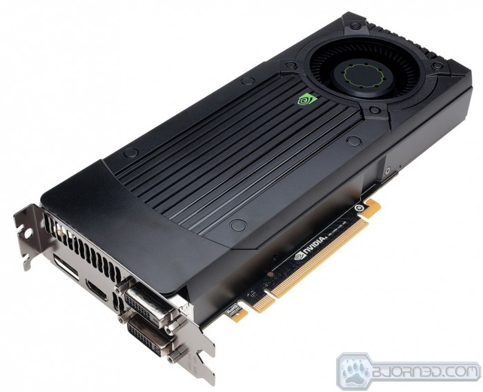
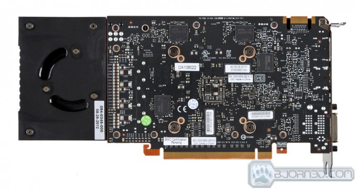
Here is the card, which looks very much like the GTX 660 (Non Ti) model card even down to the memory IC location and PCB design. Looking at the cooler as it looks to be a similar or same design i can deduct that the GTX 650 ti will have the same quiet cooling characteristics as well.
Click Images to Enlarge
The rear IO supports multiple connectivity options including:
- DVI (x2)
- HDMI
- DisplayPort
This is enough connectivity to hook up to 4 displays to this card and support a surround configuration should you have three monitors ready to game.
Click Images to Enlarge
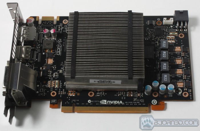
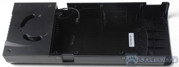
The card comes apart after many screws are removed which hold the plastic shroud and fan assembly in place. Once removed the card is much smaller than the fan assembly makes it look very much like the GTX 670, 660 and so on that we have already looked at. The cooler is a aluminum fin array much like the 670 and other cards as well from Nvidia reference design although we are sure all of the board partners will fit their own high performance cooling solutions which should further enhance the quiet properties of the card along with even better cooling.
Click Images to Enlarge
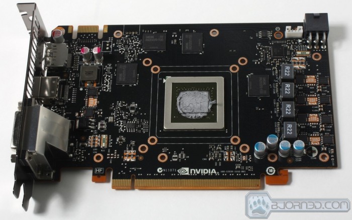
Removing the cooling fin array from the GPU was as simple as removing the four spring screws from the rear of the card. Now we can see that the cooling fin block has a copper strip running down the middle which makes direct contact with the GPU die to enhance thermal transfer.
With the cooler removed we can now confirm that the PCB and VRM design look exactly like a GTX 660 model which means it should have more than enough power to feed the GTX 650 Ti GPU.
A closer Look at the GTX 650 Ti Boost
Click Images to Enlarge
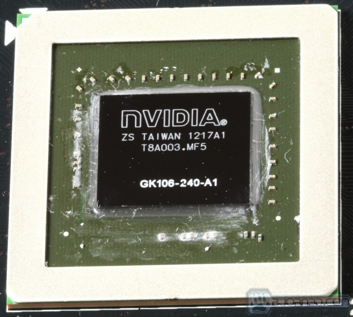
The GTX 650 Ti employs the all to familiar GK106 GPU with GPU boost for astounding performance and dynamic clocking for enhanced gaming performance.
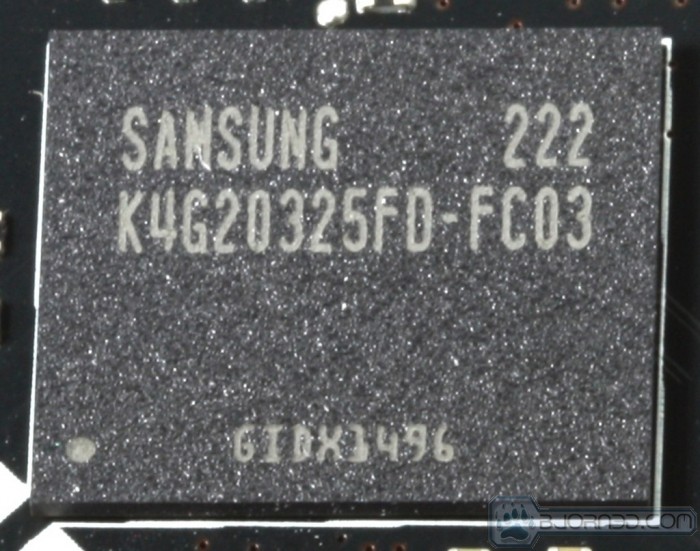
The Samsung Memory IC’s used here are rated for up to 6GHz which is right where the card is set to. These IC’s have been used on cards we have tested previously and always are capable of more but how much really depends on luck with the memory controller and IC’s, but usually you can get quite a bit more through overclocking them.
Click Images to Enlarge
Here you can see a single 6 pin is in place for power duties which is reflected in the cards 140w TDP. This should be enough for the performance of the card and even to feed it a little extra should the need to push the overclock arise. Here you can also see the GK106 GPU in relation to surrounding memory ICs.
Click Images to Enlarge
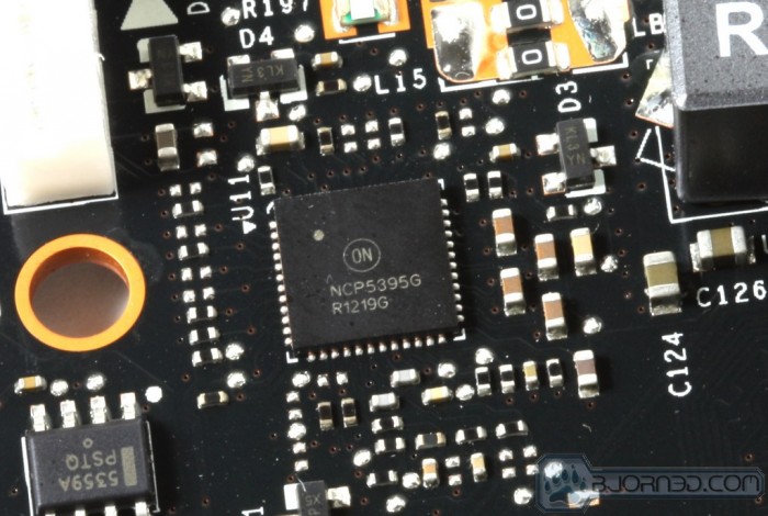
Here you see the NCP5395G controller which pushed the 4 phase VRM for the GPU on this card, and this is exactly like the GTX 660 I have seen previously, so at this point it looks like a GTX 660 PCB with GTX 650 Ti GPU fixed to it. Here even the VRM components when looking at the mosfet configuration all matches that of the layout on the GTX 660.
 Bjorn3D.com Bjorn3d.com – Satisfying Your Daily Tech Cravings Since 1996










I would add SLI support in “Pros”.
good point… and I thought I did…. thanks for the catch dude… Also keep eye out for SLI review soon… 🙂 lets see how the budget cards scale.