The long awaited Fermi GTX-480 is in the Lab. Benchmarks have been flying by like never before. GTX-480 looks very very good. Peek at the review and stop reading those rumors.
We’ve all been waiting for Fermi for so long that when it finally came through the door, it was almost like a dream. With a newly redesigned core and 3.2 Billion transistors and 512 CUDA cores (480 exposed), the GTX-480 is one cutting edge powerful GPU you won’t want to miss. The addition of DirectX capabilities and a GPU that can churn through Tessellation like no other.
Nvidia upped the ante with Nvidia Surround and Nvidia 3D Surround, and now you can span a game or application across 3 screens. Nvidia’s 3D vision has always been one of our favorite gaming methods and now you can game in 3D on three monitors. The 3D Surround (and regular Surround) will require 2 Nvidia GTX-2xx or GTX-4xx GPU’s but with the GPU power required to span across three full sized monitors, we would highly recommend GF100 (Fermi) class GPU’s.
Did Nvidia stop at adding DirectX 11 and enough hardware to make Tessellation more feasible? No, Nvidia redesigned the cache setup, tossed some heat pipes on the GTX-480, and added C++ support for CUDA. The list of improvements to GF100 goes on and on.
Nvidia took what they learned from the G90/G92 cores and applied it to GT200. Then they took what they learned from both G90 and GT200 and asked game developers what they needed, and they thoughtfully checked with the scientific community to see what those folks needed. Then they cracked out the magic 8 ball and peered into the future and made some heavy bets on the direction that GPU computing should take.
In that peek into the future they saw Tessellation, computer generated film quality gaming, extreme AA/AF setting that go up to 32x then on the 7th day they decided to toss GDDR5 on GTX-480 with a 384 bit memory buss.
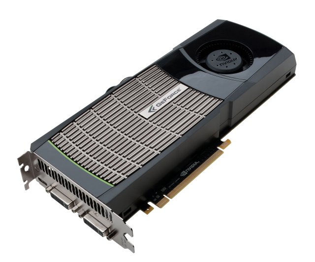
No, it’s not a photoshop composite we stole off a overseas website. No it’s not a artists rendering shot stolen off of Fudzilla it’s the real deal. It’s here and we are benching it until it screams for mercy or they stop making Red Bull. The GTX-480 is expected on E-Tailer sites soon priced at $499 USD MSRP. Discount sites might have them a little cheaper but it’s not the infamous $699 so many sites misreported in a frenzy to attract more readers at the cost of damaging their reputation.
We don’t have a GTX-470 in house right now but we have photos of one and yes they are real. Bjorn3D doesn’t play the rumor mill game. This is the real deal and it is what reference GTX-470 will look like. We have requested a GTX-470 and as soon as one hits the door, we will burn the candle at both ends to get you a review on it.
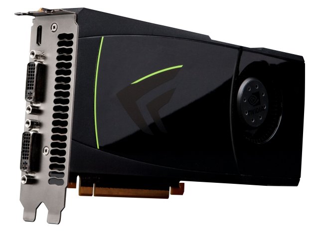
Expected to debut at $350 USD MSRP the GTX-470 combines the power of the redesigned GF100 core in a more price friendly package. With ATI’s 5850 being spotted in the $300 price range we would expect performance to top the 5850 in raw power, and with the redesigned GF100 core aimed squarely at Tessellated games and applications, it should lend itself well to heavily graphic intensive games. Both GTX-480 and GTX-470 will also run rings around any previous generation of GPUs when it comes to Ray Tracing (Sunshafts, God Rays commonly use Ray Tracing).
It’s not often a GPU brings tears to our eyes but this one did. It was that or the onions being cut in the next room we aren’t sure.
The Down and Dirty Specs on Fermi
Yes, we know you want to see the pictures of the GTX-480, but we are doing the specification and features first. Let us remind you, these are real features and specifications, not some hyped attempt at drawing more readers by speculating that Fermi was delivered by little green men. (Not Aliens the editors that let that drivel pass and turned green when they choked on it). We like the juicy, accurate, tidbit as much as the next guy but prefer solid, straight from the horses mouth information and refuse to compromise our integrity by blowing smoke up your pants leg just to increase reader hits. Call us old fashioned but the responsibility we bear to bring you accurate information actually means something to us. If you want fantasy go to the rumor rags, you want facts come to Bjorn3D.
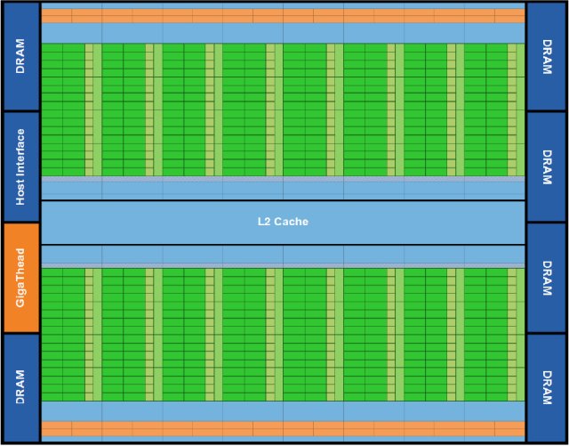
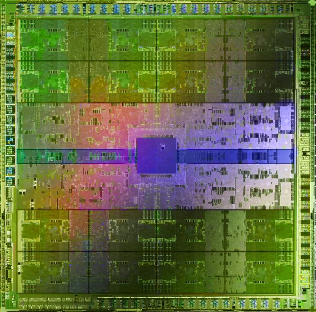
We will give you a slight break and show you a picture of Fermi’s heart, err Die.
| GPU | GTX-480 | GTX-470 | GTX-285 | 5850 | 5870 | GTX-295 | 5970 |
|---|---|---|---|---|---|---|---|
| Shader units | 480 | 448 | 240 | 1440 | 1600 | 2x 240 | 2x 1600 |
| ROPs | 48 | 40 | 32 | 32 | 32 | 2x 28 | 2x 32 |
| GPU | GF100 | GF100 | GT200b | Cypress | Cypress | 2x GT200b | 2x Cypress |
| Transistors | 3200M | 3200M | 1400M | 2154M | 2154M | 2x 1400M | 2x 2154M |
| Memory Size | 1536 MB | 1280 MB | 1024 MB | 1024 MB | 1024 MB | 2x 896 MB | 2x 1024 MB |
| Memory Bus Width | 384 bit | 320 bit | 512 bit | 256 bit | 256 bit | 2x 448 bit | 2x 256 bit |
| Core Clock | 700 MHz | 607 MHz | 648 MHz | 725 MHz | 850 MHz | 576 MHz | 725 MHz |
| Memory Clock | 924 MHz | 837 MHz | 1242 MHz | 1000 MHz | 1200 MHz | 999 MHz | 1000 MHz |
| Price | $499 | $349 | $340 | $299 | $399 | $500 | $599 |
Now we can only tell you what we were told by Nvidia on this next little tidbit, but Nvidia has never hesitated to tell us the truth and we respect them greatly for that. Rumors abound about the number of CUDA cores (Shader Units) on Fermi. The GTX-480 has 512 CUDA Cores but only 480 of those are exposed. Meaning that 32 cores are laser cut or disabled in the cards BIOS. We would suspect that they are Laser Cut but were not specifically told that.
We specifically asked (here comes the rumor part) if the 480 exposed cores were because of a manufacturing process problem. Rumors have been that due to low yeilds at the foundry only 480 cores are used. Nvidia told us in a meeting earlier this week that only 480 cores were exposed so that they could make GTX-480 more widely available to more consumers and have a wider launch pipeline. So take that for what it is. They did say that there was no problem with the fabrication process at the foundry.
We have another theory, and it’s a theory and completely constructed in our over Red Bulled brains and Nvidia hasn’t confirmed it but has hinted at it. Remember GTX-280 and GTX-260, it wasn’t long before GTX-280 was history and GTX-260 216 appeared. There is a distinct possibility that later on down the line we may see an enthusiasts enthusiast model with all 512 CUDA cores exposed. Until then we’ll have to muddle along with what, more GPU computing power than any single core GPU in the world. So when you are whining about 480 exposed cores remember those words. Most powerful single core GPU in the world.
We are sure we will hear about this but here goes. Some reports say 3.2 Billion transistors on Fermi other say 3 Billion. The information we have from Nvidia says over 3 Billion so once we get our butts chewed, we may make a minor correction to the number of transistors on the table. Right now we are 3 Red Bulls into the wind and slowing down just isn’t an option.
Straight from Nvidia’s Mouth
This next section is Nvidia’s eloquent explanation on Fermi and it’s design. We could reword it and toss in a few comments and claim it as our own but frankly that would be a disservice to the fine folks over at Nvidia that came up with it. Let’s give credit where credit is due and if we have any comments to toss in this section, they will be in bold type.
NVIDIA’s Next Generation CUDA Compute and Graphics Architecture, Code-Named “Fermi”
The Fermi architecture is the most significant leap forward in GPU architecture since the original G80. G80 was our initial vision of what a unified graphics and computing parallel processor should look like. GT200 extended the performance and functionality of G80. With Fermi, we have taken all we have learned from the two prior processors and all the applications that were written for them, and employed a completely new approach to design to create the world’s first computational GPU. When we started laying the groundwork for Fermi, we gathered extensive user feedback on GPU computing since the introduction of G80 and GT200, and focused on the following key areas for improvement:
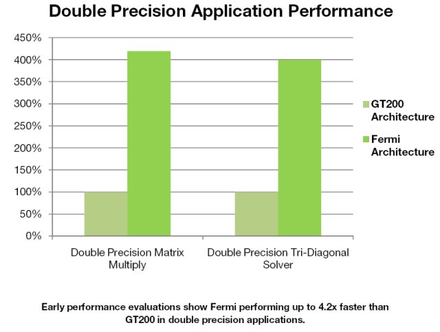
Improve Double Precision Performance—while single precision floating point performance was on the order of ten times the performance of desktop CPUs, some GPU computing applications desired more double precision performance as well.
- ECC support ECC allows GPU computing users to safely deploy large numbers of GPUs in datacenter installations, and also ensure data-sensitive applications like medical imaging and financial options pricing are protected from memory errors.
- True Cache Hierarchy some parallel algorithms were unable to use the GPU’s shared memory, and users requested a true cache architecture to aid them.
- More Shared Memory many CUDA programmers requested more than 16 KB of SM shared memory to speed up their applications.
- Faster Context Switching users requested faster context switches between application programs and faster graphics and compute interoperation.
- Faster Atomic Operations users requested faster read-modify-write atomic operations for their parallel algorithms.
With these requests in mind, the Fermi team designed a processor that greatly increases raw compute horsepower, and through architectural innovations, also offers dramatically increased programmability and compute efficiency. The key architectural highlights of Fermi are:
- Third Generation Streaming Multiprocessor (SM)
- 32 CUDA cores per SM, 4x over GT200
- 8x the peak double precision floating point performance over GT200
- Dual Warp Scheduler simultaneously schedules and dispatches instructions from tw
- independent warps
- 64 KB of RAM with a configurable partitioning of shared memory and L1 cache
- Second Generation Parallel Thread Execution ISA
- Unified Address Space with Full C++ Support
- Optimized for OpenCL and DirectCompute
- Full IEEE 754-2008 32-bit and 64-bit precision
- Full 32-bit integer path with 64-bit extensions
- Memory access instructions t
- support transition t
- 64-bit addressing
- Improved Performance through Predication
- Improved Memory Subsystem
- NVIDIA Parallel DataCacheTM hierarchy with Configurable L1 and Unified L2 Caches
- First GPU with ECC memory support
- Greatly improved atomic memory operation performance
- NVIDIA GigaThreadTM Engine
- 10x faster application context switching
- Concurrent kernel execution
- Out of Order thread block execution
- Dual overlapped memory transfer engines
An Overview of the Fermi Architecture
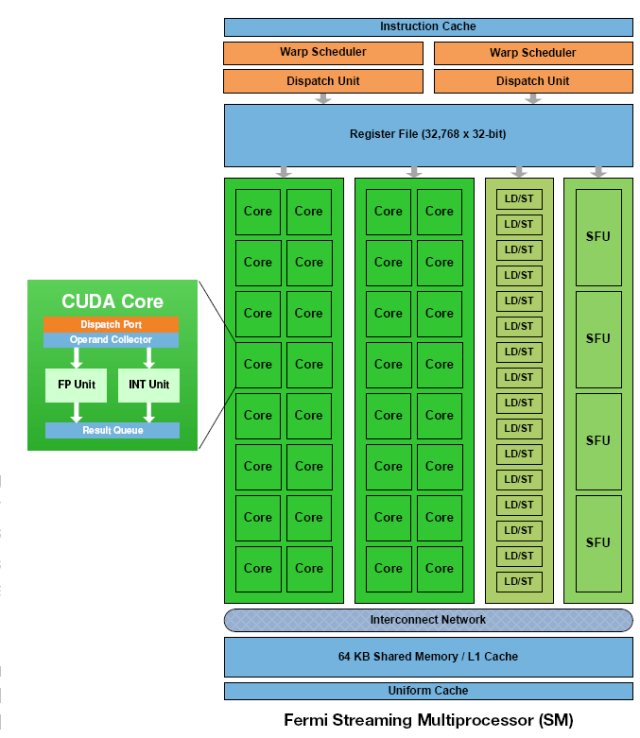
The first Fermi based GPU, implemented with 3.0 billion transistors, features up to 512 (GTX-480 has 480 cores exposed but has a total of 512 cores so we may see an enthusiast line with all 512 cores exposed at a later date, but notice the “up to 512 CUDA cores Nvidia let slip in the document) CUDA cores. A CUDA core executes a floating point or integer instruction per clock for a thread. The 512 CUDA cores are organized in 16 SMs of 32 cores each. The GPU has six 64-bit memory partitions, for a 384-bit memory interface, supporting up to a total of 6 GB of GDDR5 DRAM memory. A host interface connects the GPU to the CPU via PCI-Express. The GigaThread global scheduler distributes thread blocks to SM thread schedulers.
Third Generation Streaming Multiprocessor
The third generation SM introduces several architectural innovations that make it not only the most powerful SM yet built, but also the most programmable and efficient.
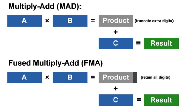
512 High Performance CUDA cores Each SM features 32 CUDA processors—a fourfold increase over prior SM designs. Each CUDA processor has a fully pipelined integer arithmetic logic unit (ALU) and floating point unit (FPU). Prior GPUs used IEEE 754-1985 floating point arithmetic. The Fermi architecture implements the new IEEE 754-2008 floating-point standard, providing the fused multiply-add (FMA) instruction for both single and double precision arithmetic. FMA improves over a multiply-add (MAD) instruction by doing the multiplication and addition with a single final rounding step, with no loss of precision in the addition. FMA is more accurate than performing the operations separately. GT200 implemented double precision FMA.
In GT200, the integer ALU was limited to 24-bit precision for multiply operations; as a result, multi-instruction emulation sequences were required for integer arithmetic. In Fermi, the newly designed integer ALU supports full 32-bit precision for all instructions, consistent with standard programming language requirements. The integer ALU is also optimized to efficiently support 64-bit and extended precision operations. Various instructions are supported, including Boolean, shift, move, compare, convert, bit-field extract, bit-reverse insert, and population count.
16 Load/Store Units
Each SM has 16 load/store units, allowing source and destination addresses to be calculated for sixteen threads per clock. Supporting units load and store the data at each address to cache or DRAM.
Four Special Function Units
Special Function Units (SFUs) execute transcendental instructions such as sin, cosine, reciprocal, and square root. Each SFU executes one instruction per thread, per clock; a warp executes over eight clocks. The SFU pipeline is decoupled from the dispatch unit, allowing the dispatch unit to issue to other execution units while the SFU is occupied.
Fermi’s 16 SM are positioned around a common L2 cache. Each SM is a vertical rectangular strip that contain an orange portion (scheduler and dispatch), a green portion (execution units), and light blue portions (register file and L1 cache).
The Down and Dirty Specs on Fermi Cont.
Designed for Double Precision
Double precision arithmetic is at the heart of HPC applications such as linear algebra, numerical simulation, and quantum chemistry. The Fermi architecture has been specifically designed to offer unprecedented performance in double precision; up to 16 double precision fused multiply-add operations can be performed per SM, per clock, a dramatic improvement over the GT200 architecture.
Dual Warp Scheduler
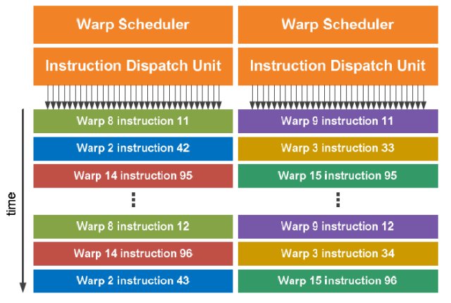
The SM schedules threads in groups of 32 parallel threads called warps. Each SM features two warp schedulers and two instruction dispatch units, allowing two warps to be issued and executed concurrently. Fermi’s dual warp scheduler selects two warps, and issues one instruction from each warp to a group of sixteen cores, sixteen load/store units, or four SFUs. Because warps execute independently, Fermi’s scheduler does not need to check for dependencies from within the instruction stream. Using this elegant model of dual-issue, Fermi achieves near peak hardware performance.
Most instructions can be dual issued; two integer instructions, two floating instructions, or a mix of integer, floating point, load, store, and SFU instructions can be issued concurrently. Double precision instructions do not support dual dispatch with any other operation. (Someone at Nvidia must have let that slip by because previous to today we thought that SFU meant “Shut the Frack Up”.)
64 KB Configurable Shared Memory and L1 Cache
One of the key architectural innovations that greatly improved both the programmability and performance of GPU applications is on-chip shared memory. Shared memory enables threads within the same thread block to cooperate, facilitates extensive reuse of on-chip data, and greatly reduces off-chip traffic. Shared memory is a key enabler for many high-performance CUDA applications.
G80 and GT200 have 16 KB of shared memory per SM. In the Fermi architecture, each SM has 64 KB of on-chip memory that can be configured as 48 KB of Shared memory with 16 KB of L1 cache or as 16 KB of Shared memory with 48 KB of L1 cache.
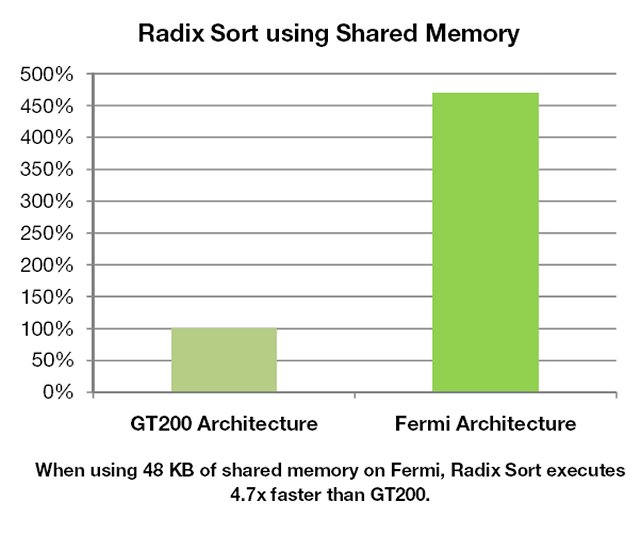
For existing applications that make extensive use of Shared memory, tripling the amount of Shared memory yields significant performance improvements, especially for problems that are bandwidth constrained. For existing applications that use Shared memory as software managed cache, code can be streamlined to take advantage of the hardware caching system, while still having access to at least 16 KB of shared memory for explicit thread cooperation. Best of all, applications that do not use Shared memory automatically benefit from the L1 cache, allowing high performance CUDA programs to be built with minimum time and effort.
Second Generation Parallel Thread Execution ISA
Fermi is the first architecture to support the new Parallel Thread eXecution (PTX) 2.0 instruction set. PTX is a low level virtual machine and ISA designed to support the operations of a parallel thread processor. At program install time, PTX instructions are translated to machine instructions by the GPU driver.
The primary goals of PTX are:
- Provide a stable ISA that spans multiple GPU generations
- Achieve full GPU performance in compiled applications
- Provide a machine-independent ISA for C, C++, Fortran, and other compiler targets.
- Provide a code distribution ISA for application and middleware developers
- Provide a common ISA for optimizing code generators and translators, which map PTX to specific target machines.
- Facilitate hand-coding of libraries and performance kernels
- Provide a scalable programming model that spans GPU sizes from a few cores to many
PTX 2.0 introduces several new features that greatly improve GPU programmability, accuracy, and performance. These include: full IEEE 32-bit floating point precision, unified address space for all variables and pointers, 64-bit addressing, and new instructions for OpenCL and DirectCompute. Most importantly, PTX 2.0 was specifically designed to provide full support for the C++ programming language.
Unified Address Space enables Full C++ Support
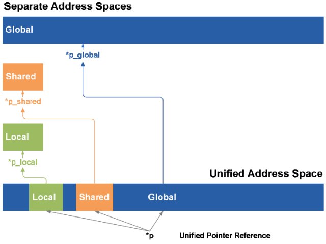
Fermi and the PTX 2.0 ISA implement a unified address space that unifies the three separate address spaces (thread private local, block shared, and global) for load and store operations. In PTX 1.0, load/store instructions were specific to one of the three address spaces; programs could load or store values in a specific target address space known at compile time. It was difficult to fully implement C and C++ pointers since a pointer’s target address space may not be known at compile time, and may only be determined dynamically at run time.
With PTX 2.0, a unified address space unifies all three address spaces into a single, continuous address space. A single set of unified load/store instructions operate on this address space, augmenting the three separate sets of load/store instructions for local, shared, and global memory. The 40-bit unified address space supports a Terabyte of addressable memory, and the load/store ISA supports 64-bit addressing for future growth.
The implementation of a unified address space enables Fermi to support true C++ programs. In C++, all variables and functions reside in objects which are passed via pointers. PTX 2.0 makes it possible to use unified pointers to pass objects in any memory space, and Fermi’s hardware address translation unit automatically maps pointer references to the correct memory space
Fermi and the PTX 2.0 ISA also add support for C++ virtual functions, function pointers, and ‘new’ and ‘delete’ operators for dynamic object allocation and de-allocation. C++ exception handling operations ‘try’ and ‘catch’ are also supported.
Optimized for OpenCL and DirectCompute
OpenCL and DirectCompute are closely related to the CUDA programming model, sharing the key abstractions of threads, thread blocks, grids of thread blocks, barrier synchronization, perblock shared memory, global memory, and atomic operations. Fermi, a third-generation CUDA architecture, is by nature well-optimized for these APIs. In addition, Fermi offers hardware support for OpenCL and DirectCompute surface instructions with format conversion, allowing graphics and compute programs to easily operate on the same data. The PTX 2.0 ISA also adds support for the DirectCompute instructions population count, append, and bit-reverse.
IEEE 32-bit Floating Point Precision
Single precision floating point instructions now support subnormal numbers by default in hardware, as well as all four IEEE 754-2008 rounding modes (nearest, zero, positive infinity, and negative infinity).
Subnormal numbers are small numbers that lie between zero and the smallest normalized number of a given floating point number system. Prior generation GPUs flushed subnormal operands and results to zero, incurring a loss of accuracy. CPUs typically perform subnormal calculations in exception-handling software, taking thousands of cycles. Fermi’s floating point units handle subnormal numbers in hardware, allowing values to gradually underflow to zero with no performance penalty.
A frequently used sequence of operations in computer graphics, linear algebra, and scientific applications is to multiply two numbers, adding the product to a third number, for example, D = A × B + C. Prior generation GPUs accelerated this function with the multiply-add (MAD) instruction that allowed both operations to be performed in a single clock. The MAD instruction performs a multiplication with truncation, followed by an addition with round-to-nearest even. Fermi implements the new fused multiply-add (FMA) instruction for both 32-bit single-precision and 64-bit double-precision floating point numbers (GT200 supported FMA only in double precision) that improves upon multiply-add by retaining full precision in the intermediate stage. The increase in precision benefits a number of algorithms, such as rendering fine intersecting geometry, greater precision in iterative mathematical calculations, and fast, exactly-rounded division and square root operations.
Improved Conditional Performance through Predication
In the Fermi ISA, the native hardware predication support used for divergent thread management is now available at the instruction level. Predication enables short conditional code segments to execute efficiently with no branch instruction overhead.
Memory Subsystem Innovations
NVIDIA Parallel DataCacheTM with Configurable L1 and Unified L2 Cache
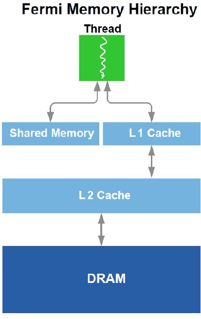
Working with hundreds of GPU computing applications from various industries, we learned that while Shared memory benefits many problems, it is not appropriate for all problems. Some algorithms map naturally to Shared memory, others require a cache, while others require a combination of both. The optimal memory hierarchy should offer the benefits of both Shared memory and cache, and allow the programmer a choice over its partitioning. The Fermi memory hierarchy adapts to both types of program behavior.
Adding a true cache hierarchy for load / store operations presented significant challenges. Traditional GPU architectures support a read-only ‘‘load’’ path for texture operations and a write-only ‘‘export’’ path for pixel data output. However, this approach is poorly suited to executing general purpose C or C++ thread programs that expect reads and writes to be ordered. As one example: spilling a register operand to memory and then reading it back creates a read after write hazard; if the read and write paths are separate, it may be necessary to explicitly flush the entire write / ‘‘export’’ path before it is safe to issue the read, and any caches on the read path would not be coherent with respect to the write data.
The Fermi architecture addresses this challenge by implementing a single unified memory request path for loads and stores, with an L1 cache per SM multiprocessor and unified L2 cache that services all operations (load, store and texture). The per-SM L1 cache is configurable to support both shared memory and caching of local and global memory operations. The 64 KB memory can be configured as either 48 KB of Shared memory with 16 KB of L1 cache, or 16 KB of Shared memory with 48 KB of L1 cache. When configured with 48 KB of shared memory, programs that make extensive use of shared memory (such as electrodynamic simulations) can perform up to three times faster. For programs whose memory accesses are not known beforehand, the 48 KB L1 cache configuration offers greatly improved performance over direct access to DRAM.
In either configuration, the L1 cache also helps by caching temporary register spills of complex programs. Prior generation GPUs spilled registers directly to DRAM, increasing access latency. With the L1 cache, performance scales gracefully with increased temporary register usage.
Fermi features a 768 KB unified L2 cache that services all load, store, and texture requests. The L2 provides efficient, high speed data sharing across the GPU. Algorithms for which data addresses are not known beforehand, such as physics solvers, raytracing, and sparse matrix multiplication especially benefit from the cache hierarchy. Filter and convolution kernels that require multiple SMs to read the same data also benefit.
First GPU with ECC Memory Support
Fermi is the first GPU to support Error Correcting Code (ECC) based protection of data in memory. ECC was requested by GPU computing users to enhance data integrity in high performance computing environments. ECC is a highly desired feature in areas such as medical imaging and large-scale cluster computing.
Naturally occurring radiation can cause a bit stored in memory to be altered, resulting in a soft error. ECC technology detects and corrects single-bit soft errors before they affect the system. Because the probability of such radiation induced errors increase linearly with the number of installed systems, ECC is an essential requirement in large cluster installations.
Fermi supports Single-Error Correct Double-Error Detect (SECDED) ECC codes that correct any single bit error in hardware as the data is accessed. In addition, SECDED ECC ensures that all double bit errors and many multi-bit errors are also be detected and reported so that the program can be re-run rather than being allowed to continue executing with bad data.
Fermi’s register files, shared memories, L1 caches, L2 cache, and DRAM memory are ECC protected, making it not only the most powerful GPU for HPC applications, but also the most reliable. In addition, Fermi supports industry standards for checking of data during transmission from chip to chip. All NVIDIA GPUs include support for the PCI Express standard for CRC check with retry at the data link layer. Fermi also supports the similar GDDR5 standard for CRC check with retry (aka “EDC”) during transmission of data across the memory bus.
Fast Atomic Memory Operations
Atomic memory operations are important in parallel programming, allowing concurrent threads to correctly perform read-modify-write operations on shared data structures. Atomic operations such as add, min, max, and compare-and-swap are atomic in the sense that the read, modify, and write operations are performed without interruption by other threads. Atomic memory operations are widely used for parallel sorting, reduction operations, and building data structures in parallel without locks that serialize thread execution.
Thanks to a combination of more atomic units in hardware and the addition of the L2 cache, atomic operations performance is up to 20× faster in Fermi compared to the GT200 generation.
GigaThreadTM Thread Scheduler
One of the most important technologies of the Fermi architecture is its two-level, distributed thread scheduler. At the chip level, a global work distribution engine schedules thread blocks to various SMs, while at the SM level, each warp scheduler distributes warps of 32 threads to its execution units. The first generation GigaThread engine introduced in G80 managed up to 12,288 threads in realtime. The Fermi architecture improves on this foundation by providing not only greater thread throughput, but dramatically faster context switching, concurrent kernel execution, and improved thread block scheduling.
10x Faster Application Context Switching
Like CPUs, GPUs support multitasking through the use of context switching, where each program receives a time slice of the processor’s resources. The Fermi pipeline is optimized to reduce the cost of an application context switch to below 25 microseconds, a significant improvement over last generation GPUs. Besides improved performance, this allows developers to create applications that take greater advantage of frequent kernel-to-kernel communication, such as fine-grained interoperation between graphics and PhysX applications.
Concurrent Kernel Execution
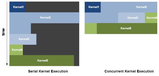
Fermi supports concurrent kernel execution, where different kernels of the same application context can execute on the GPU at the same time. Concurrent kernel execution allows programs that execute a number of small kernels to utilize the whole GPU. For example, a PhysX program may invoke a fluids solver and a rigid body solver which, if executed sequentially, would use only half of the available thread processors. On the Fermi architecture, different kernels of the same CUDA context can execute concurrently, allowing maximum utilization of GPU resources. Kernels from different application contexts can still run sequentially with great efficiency thanks to the improved context switching performance.
Conclusion
For sixteen years, NVIDIA has dedicated itself to building the world’s fastest graphics processors. While G80 was a pioneering architecture in GPU computing, and GT200 a major refinement, their designs were nevertheless deeply rooted in the world of graphics. The Fermi architecture represents a new direction for NVIDIA. Far from being merely the successor to GT200, Fermi is the outcome of a radical rethinking of the role, purpose, and capability of the GPU.
Rather than taking the simple route of adding execution units, the Fermi team has tackled some of the toughest problems of GPU computing. The importance of data locality is recognized through Fermi’s two level cache hierarchy and its combined load/store memory path. Double precision performance is elevated to supercomputing levels, while atomic operations execute up to twenty times faster. Lastly, Fermi’s comprehensive ECC support strongly demonstrates our commitment to the high-performance computing market.
On the software side, the architecture brings forward support for C++, the world’s most ubiquitous object-orientated programming language, and Nexus, the world’s first integrated development environment designed for massively parallel GPU computing applications.
With its combination of ground breaking performance, functionality, and programmability, the Fermi architecture represents the next revolution in GPU computing.
Pictures
GTX-480

We are leading out with a shot of the GTX-480 chip because later on the page, we have beauty shots of the GTX-470, and the chip shots help to avoid that confusion between the GTX-480 and it’s little brother the GTX-470.

Superficially, the GTX-480 looks much like previous generations of Nvidia GPU’s, but Nvidia incorporated a raised surface on part of the cards cowling. The raised design is likely to aid in cooling this massively powerful GPU.
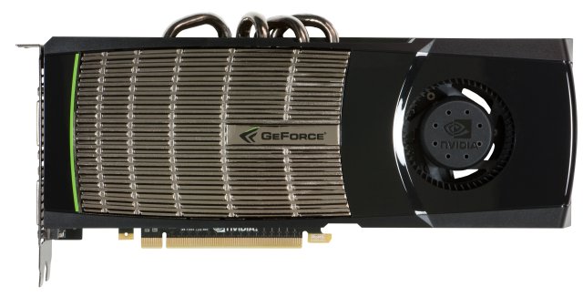
We’ve seen aftermarket GPU’s with heatpipes but the GTX-480 reference model has 4 heat pipes protruding from its sleek top. Like all current Nvidia GPU’s the GTX-480 uses a PCI-E 16x slot and this beauty takes an 8 pin and 6 pin PCI-E power connector, and max power pull is rated at 250 watts. A minimum PSU (of good quality not a flea market PSU) rated at 600w is recommended for the GTX-480.
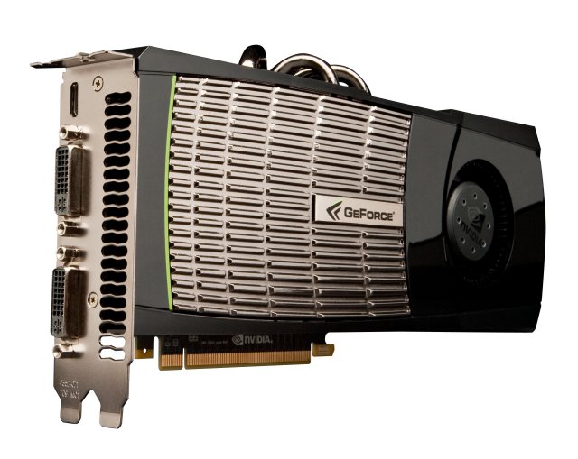
GTX-480 sports a pretty normal looking squirrel cage fan but we’ve seen it (In GPU-Z) running at 5000+ RPM so they may have beefed the fan up a little. The card has a normal dual slot design with vent for exhausting some of the heat this behemoth is sure to generate outside the chassis. Two DVI-D ports and a Mini HDMI reside on the GTX-480 and the Mini HDMI is a little too close to the top card for our tastes.
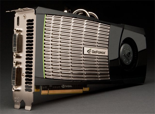
We decided to include a black background shot of the 480 because it shows the small green highlight on the front of the card well, so look and drool. Drool towels are available in the vending machine for the nominal cost of $29.95.
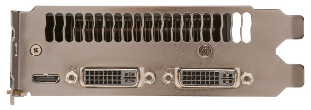
Here’s a shot of the GTX-480’s expansion port cover plate and you can see how close to the top of the card the Mini HDMI really is. You can connect to it but you may have to be looking directly at it to get it connected. With the massive GPU computing power of the GTX-480 and a 250W maximum power consumption we would suspect that the Mini HDMI needed to be on top the card so that it can have a full length heat exhaust. Face it the GTX-480 has to dissipate 250W of thermal energy from a 529mm² surface area. ATI’s top GPU (single core) the 5870 has a die size of 330mm² and packs over 2 billion transistors. Apparently Nvidia needed the extra 200mm² for all the new features they implemented. This is one behemoth die size and it’s dissipating 250w of thermal energy at peak load. She be one hot mama but you can bet in games she gives good sugar.
GTX-470
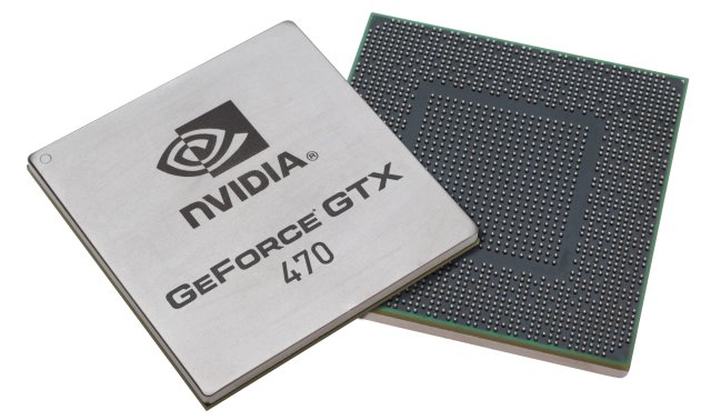
Like we mentioned we included chip shots of the GTX-470 because we put the pictures on the same page. We do not have a GTX-470 in house at this time, but we didn’t want to deny you the chance to take a gander at one, so we included them as a courtesy.
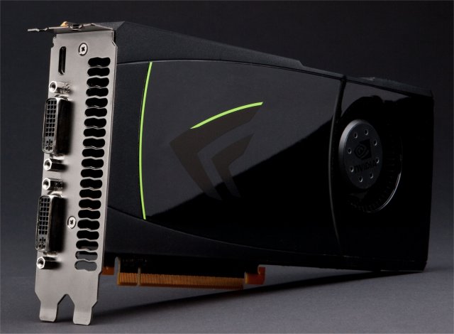
We resorted to our black background for one shot on the GTX-470 so the white background doesn’t overpower the subtle green accents on the card. With a white background it was just too washed out.
Now, the more astute among you should notice one major difference between the 480 and the 470. No it’s not the absence of a perforated side although that is missing on the GTX-470. There are no heatpipes on the GTX-470 that extend beyond the cowling like the GTX-480 has.
Let’s think a little here, the GTX-480 has 480 exposed cores, and the GTX-470 has 448 exposed cores. The GTX-480 needs heat pipes that extend beyond the cowling and the GTX-470 doesn’t need them. This is entirely speculation but the GTX-480 may have 480 exposed cores instead of 512 because 512 cores might have exceeded the viable thermal envelope of a dual slot cooler design. If that is the case we would have rather seen a dual fan cowling design with all 512 cores exposed. One thing you can bet on GTX-480 is one hot runner and aftermarket cooled cards will be all the rage.

The GTX-470 looks much more familiar than the GTX-480 with it’s heat pipes. There’s little on the exterior design that will distinguish the GTX-470 from a GTX-275 from a cosmetic standpoint.
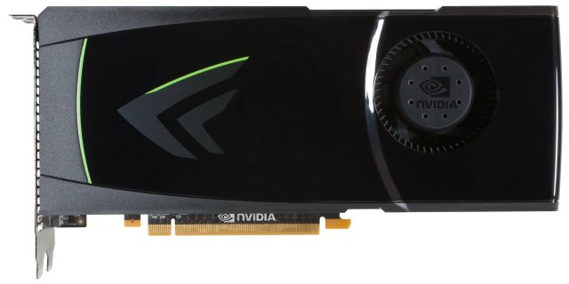
Standard squirrel cage fan and PCI-E 16x connector. The GTX-470 uses two 6 pin PCI-E power connectors and requires a GOOD QUALITY 550W PSU. Maximum power draw is rated at 215W. Lets do a little paper napkin math here. Paper napkin math is the type you can wad up and throw away if you don’t like so take it for what it’s worth and keep those emails out of my inbox. GTX-480 has 480 cores and needs max power of 250w. GTX-470 has 448 cores exposed and that’s 32 fewer cores than GTX-480. GTX-480 has 32 cores un-exposed and it makes sense that an Ultra GTX-480 or GTX-512 whatever it may or may not be called if one appears should need 285w maximum.
Now lets do a little more napkin math. Two 6 pin PCI-E power connectors provide 150W, PCI-E slot provides 75W totaling 225W. Enough for GTX-470 with a little room for overclocking but not enough for GTX-480. GTX-480 has one PCI-E 8 pin for 150W and one PCI-E 6 pin for 75W and PCI-E slot for 75W. That totals 300w. So add 32 cores to GTX-480 for 512 CUDA cores and it needs 285W. So exposing all 512 cores without a PCB redesign is feasible. Coincidence or shrewd planning, you make the call. More than likely 512 core models would use two 8 pin to avoid drawing so much power from the PCI-E slot but it should be doable with one 6 and one 8 pin PCI-E.

The GTX-470 has the same port design that we described for the GTX-480.
GF100 Design & Why
At some point in technology, you have to look at what the end user wants, and what the vendors providing the technology are giving. Often you find technology partners saying, here’s what we have, and here’s what you are limited to doing with it. By the same token, hardware developers have to look at where the industry is going and plan for giving what the developers need to give the end user more. With manufacturing technology advancing almost as fast as the desire for it, hardware vendors are looking more at what the hardware needs to do the job more efficiently and to deliver a more targeted product to adhere to today’s needs.
Nvidia is no exception to that cycle. They are however well tuned to the wants and needs of both developers and end users. To that end, the technology packaged in Fermi (GF100) is tailored to today’s needs and not just a more powerful refresh of the GT200 core. You can get more raw power by tossing more transistors and hardware at the problem, but if that raw power doesn’t do the job it needs, then it’s just wasted raw power. Fermi addresses raw power but it’s more focused to doing what it needs to do to deliver a great end user/developer platform than previous Nvidia cores. Nvidia uses this concept to make a great core into a newer shinier redesigned core that delivers more raw power and the ability to excel at exactly what games need.
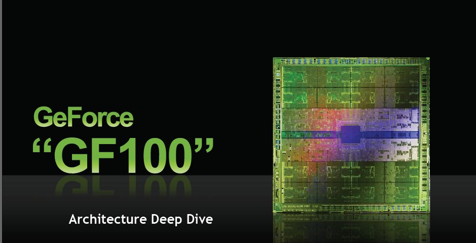
Like usual, the first slide in the deck is just and introduction to the topic heading and of course a cool peek at the core itself.
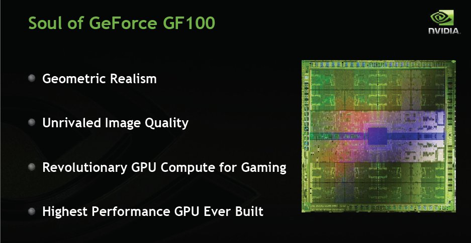
This slide lets us know what Fermi is targeting. First and high on the scale of importance, Geometric Realism. If you’ve been paying attention, that’s usually accomplished with tons and tons of triangles hung as wireframes. Previous generations of GPU’s were serial triangle producers and could only generate one triangle per clock cycle. Fermi can theoretically produce 4 but in reality it can parallel produce 2.5 – 2.7 triangles per clock cycle. Tessellation takes the triangles on a wire frame and breaks the larger triangles into smaller triangles, and that increased the load on the geometric portion of the GPU, and was creating a bottleneck. Fermi parallel produces triangles and is Nvidia’s solution to that bottleneck.
Tessellation is by no means a new technology but game developers can’t produce Film like Tessellation because of the limitations of the geometry portion of existing GPU’s. Special effect houses for the film industry often use millions of triangles per frame, they however have the advantage of being able to spend copious time on each frame. GPU’s have a fraction of a second to render a whole frame and the Parallel geometry processing of Fermi is exactly what the game developers need to produce a more film like polished game.
This is, of course, a large investment and gamble on Nvidia’s part. How many of the technologies of yesteryear are still around. Game developers have to pick up Tessellation and utilize it or the gamble may not pay off. We’ve seen Tessellation in action and if game developers don’t adopt it then they obviously need professional help. Speaking of Tessellation check out the YouTube of Hair Tessellation we’ve linked in below.
In a lot of games, you see a profusion of hats and bald people, hair is very hard to simulate and it’s GPU Tesselation and PhysX intensive. You can imagine the number of hairs on your head and making them react naturally with the surrounding environment (and looking real) and how hard that would be for a CPU or GPU to make look real. It’s still GPU intensive but Fermi’s design might end up being the Rogaine of computer technology. Hopefully we’ll be seeing fewer hats and plastic hair in the near future.
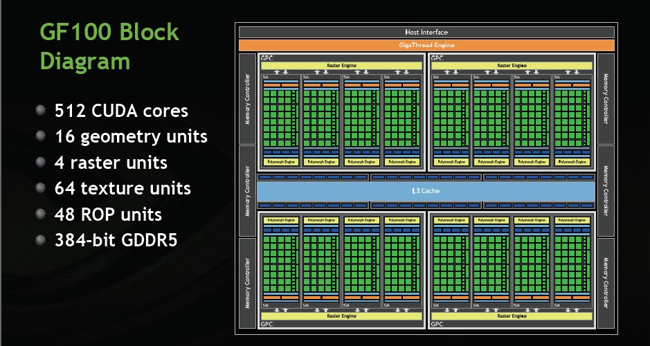
Fermi (GF100) features 512 CUDA Cores, 16 Geometry units, 4 Raster Units, 64 texture units, 48 ROP units and sports a 384 bit memory bus fed by GDDR5 memory. Previous top end Nvidia GPU’s had a wider 512bit Bus for GDDR3 memory. GDDR5 is faster so they can get away with a narrower bus. Compared to the AMD setup on top end GPUs, this is pretty generous. ATI has a 256bit bus for GDDR5, Nvidia is driving 50% more memory bus on the same GDDR5. We ask about the narrower bus on Fermi and faster GDDR5 and a wider bus would have made it more expensive was the answer we got.
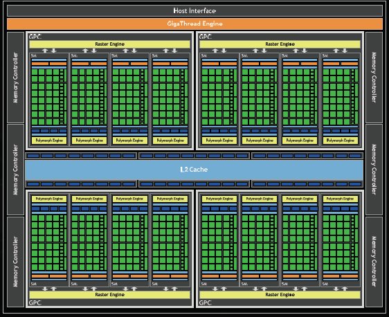
For those among you that drool over block diagrams, we included a little bigger shot of the design.
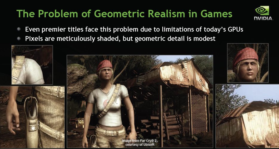
Now take a look at the gun holster in the bottom left pane in this shot and you can see that instead of being naturally rounded like leather holsters are, it has a little geometric angling. That’s a trade off between power available and desired detail. Fermi is designed to address this exact problem. Notice the traditional bandanna covering the expected plastic hair.
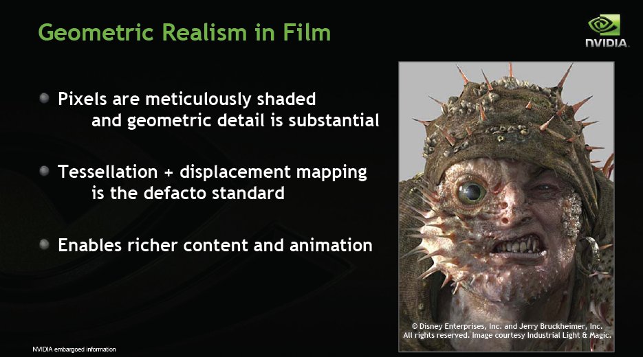
Now take this guy from Pirates of the Caribbean produced in a film studio where each frame is carefully Tessellated and displacement mapping is the defacto standard. Of course like we mentioned earlier, the studio can spend hours on one frame while the GPU has a fraction of a second to do the same thing. The end result of the heavy Tessellation and displacement mapping is a much more realistic character which is required for film to make it more believable and realistic. GPU’s starting with Fermi are moving that direction and with it’s massively increased raw power and laser focus on geometric realism, Nvidia GPU’s are heading for more realistic film like gaming. With GPU power doubling about every 12 months it shouldn’t be long before we see film like video games if the game developers are up to the task.
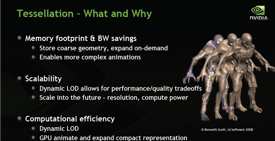
Tessellation, like we explained earlier, is the process of using triangles for wireframe designs. Back in the day some called it polygon processing and games with it featured very angled unrealistic surfaces and creatures. GPU’s have vastly improved since then and they still use triangles for wire frames but they use a lot more of them now than back in the fledgling days of polygon programming. Tessellation is a major improvement on polygon wireframes, it takes the triangles on a wireframe and breaks them down into a multitude of smaller triangles, making the image look smoother and rounder. With that increase in the number of triangles you increase the bottleneck of the previous generations serial production of triangles. Fermi, like we mentioned before, is the first GPU designed to parallel produce the triangles decreasing that bottleneck dramatically. We say decreasing because if hardware vendors deliver it game developers can overwhelm it (Think Crysis).
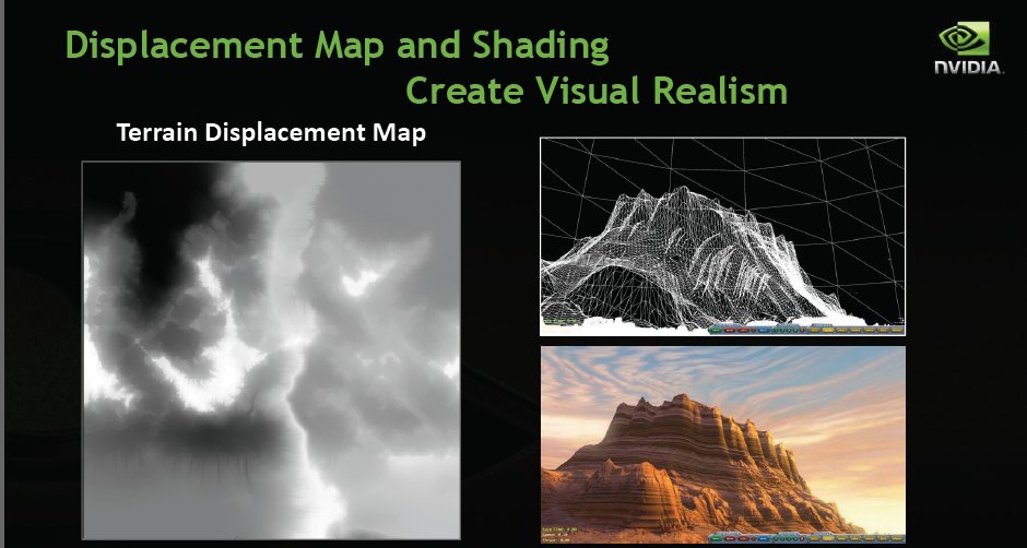
Displacement mapping, this is a hard concept unless you’ve studied it a little. Displacement mapping allows game developers to take what would be a flat pattern on the screen and give it depth or projection. To raise or lower a surfaces appearance. See the example below.
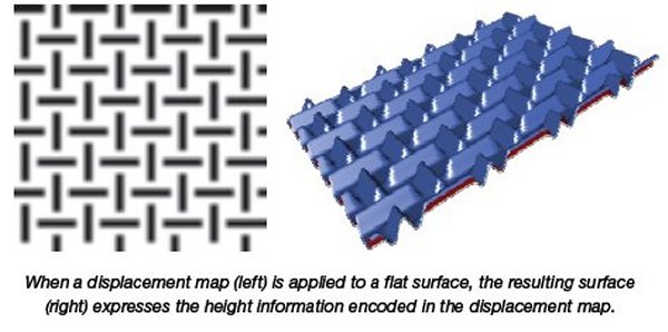
In the example you can see the raised surface created from displacement mapping. What that means to gaming is that flat surfaces with a shaded skin can now give a more realistic appearance of being raised. Move on to the next image and you get to see a better example.
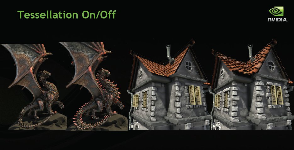
Now in this slide the dragon on the left looks decent but it’s probably not what the artist had envisioned as optimal. Apply Tessellation and displacement mapping and you get the dragon on the right which looks more like what we envision a dragon should look like. The house on the right the roof looks flat and is nothing more than a painted on skin, apply tessellation and you get raised roof tiles. Small changes that make a big difference to the eye.
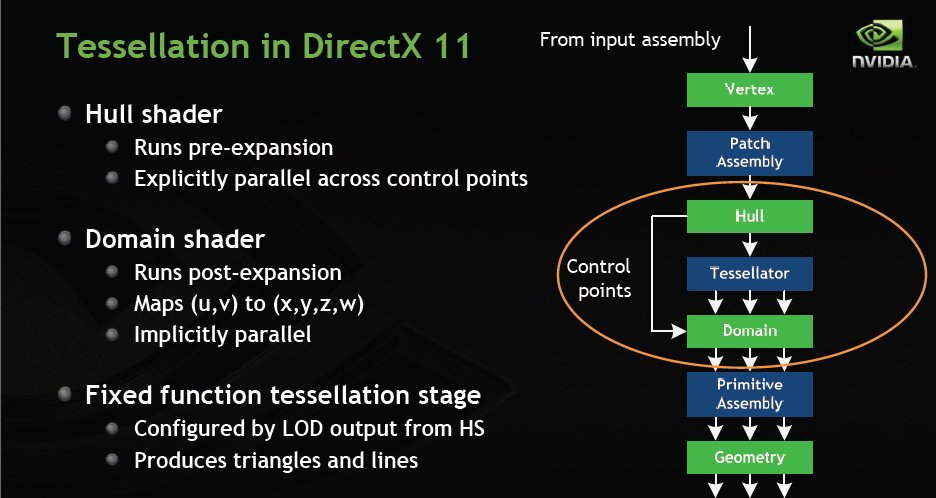
Here’s the block diagram of Tessellation in DX11. The data flows from the Vertex to the patch assembly then to the Hull where the Tesselator takes over if needed. At that point processing becomes parallel and remains parallel through the rest of the workflow. If Tessellation isn’t required, Tesselator is bypassed and data moves on to the Domain and on to the Primitive assembly and finally on to the Geometry engine. The diagram is a little deceptive because it downplays one of Fermi’s evolutionary leaps, parallel triangle production.
All of that talk about Tessellation is fine and good but check out the Tessellation Water Demo we linked in and you can see the real benefit of Tessellation. Keep in mind that it’s scalable to the amount of processing power you have, Once you’ve seen the video we think that you will understand why Tessellation and FERMI being designed for the growth of Tessellation in the game development industry is so important. You might also want to keep in mind wire frames and those tons and tons of triangles Fermi is so good at producing.

Now here’s the rough of it. Adding Tessellation to GT200 core GPU’s you get a bottleneck.GT200 had single triangle capabilities like all previous GPU’s (Nvidia and ATI and despite ATI’s loose word play about producing two triangles on 5xxx GPU’s in reality they just improved serial triangle production so if you fell for the 5xxx dual triangle production ATI hinted at we are here to tell you it’s still serial (single) triangle production).
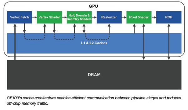
Fermi got a shared L2 cache (768KB configurable) that drastically decreases the off die transport of data.
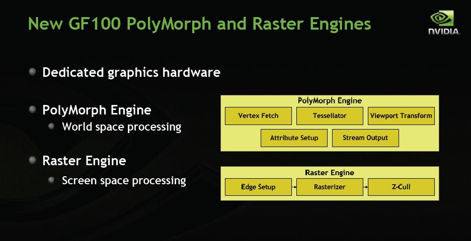
Fermi also gets a redesigned PolyMorph and Raster Engine setup.
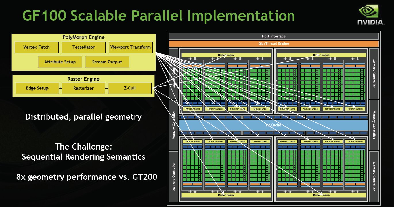
Here’s what we have been hammering all along Distributed Parallel geometry processing. Fermi sports 8x the geometry performance of GT200.
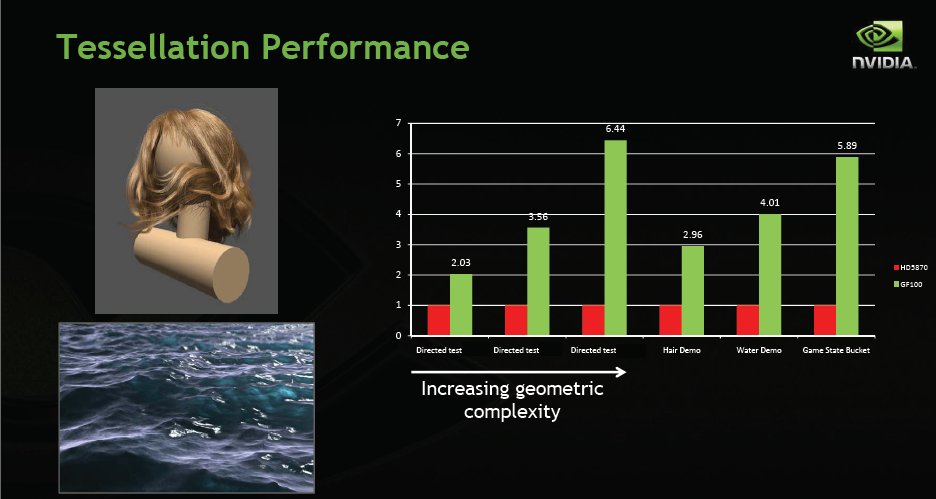
We saw the hair demo earlier and the Water demo is a little closer in the memory. The red bars are using ATI 5870 performance as 100% the green bars are Fermi GF100 (full blown top end Fermi) and you can clearly see that in Tessellation in these examples is light years ahead of the 5xxx lineup. It follows that since so much of game development is in fact geometric programming (wireframes/triangles and now tessellation) that Fermi is going to be a monster GPU capable of producing an end user experience like nothing we have ever seen.
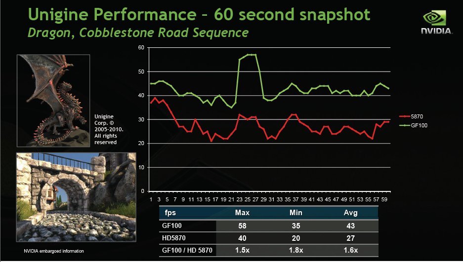
In Unigines bench using a 60 second snapshot Fermi’s performance ranged from 1.5x to 1.8x the performance of the 5870. Results will vary and shader and geometry heavy games will show Fermi’s true power.

Geometry shader performance on Fermi is off the map. Again using ATI 5870 for a reference as 100% Fermi is topping that by a factor of 4 – 4.7x.
Fermi for Gaming
As we all know, Nvidia’s bread and butter is gaming and not just gaming but improving and driving the cutting edge of gaming. The Nvidia philosophy of delivering the best possible end user experience drives their concepts and designs for their GPU’s. With that kind of commitment it’s no surprise that Fermi is a laser precise answer to today’s gaming needs and it’s design is meant to carry GPU design and gaming into to future.
As usual the first slide from the deck is just introducing the topic.
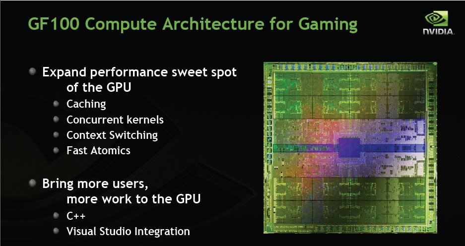
Fermi brings a lot to the table and it features new caching and a shared configurable L2 cache, concurrent kernels, context switching, and fast atomics. It also has support for C++ and Visual studio integration.
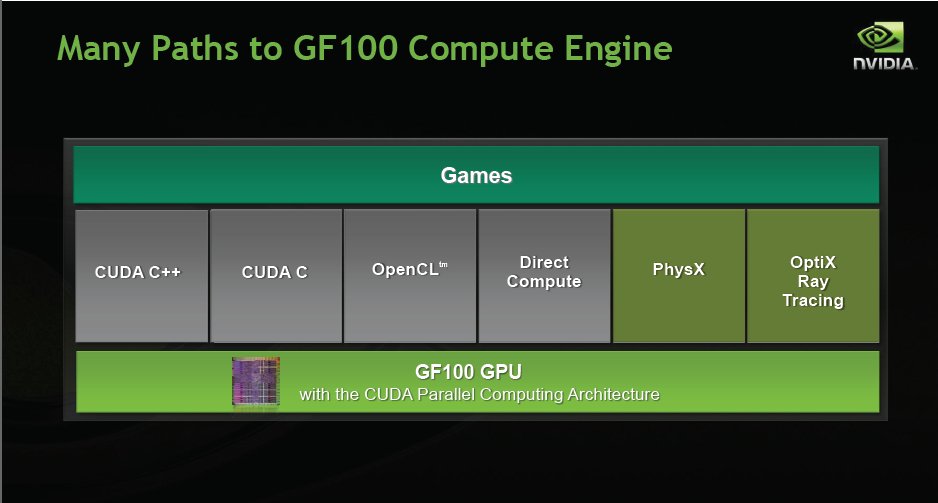
A lot of people when they think of CUDA think folding but it’s more than just that. Nvidia has expanded support to C++ and still supports C, OpenCL, Direct Compute, proprietary PhysX and OptiX Ray Tracing.
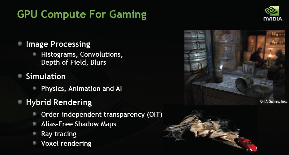
Gaming specifically we get histograms, convolutions, depth of field, and motion blurs as well as static blurs. People think blur why would we want blurs. That’s the way the human eye works, we focus on one point or area and anything beyond that point blurs. Motion wise if something moves to fast our eyes can’t see it but the brain fills in the gaps and we see a blur.
For simulations Fermi brings Physics animation and AI. Physics (PhysX) brings more realism through increased destruction of in game materials and realism through accurate calculation of how things will act. AI has been an issue for a while, put to much AI into a game and things bog down. Fermi can help relieve that problem and allow for more in game AI’s to dispatch.
Fermi also offers Hybrid Rendering in the form of Order-independent transparency (OIT), Alias-Free Shadow Maps, Ray Tracing, and Voxel rendering.
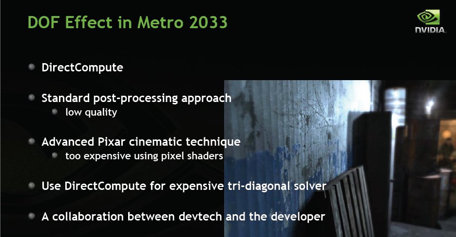
What does a lot of that add up to. A sharp image in the foreground blending seamlessly to a blurred background. (Including but not limited to)
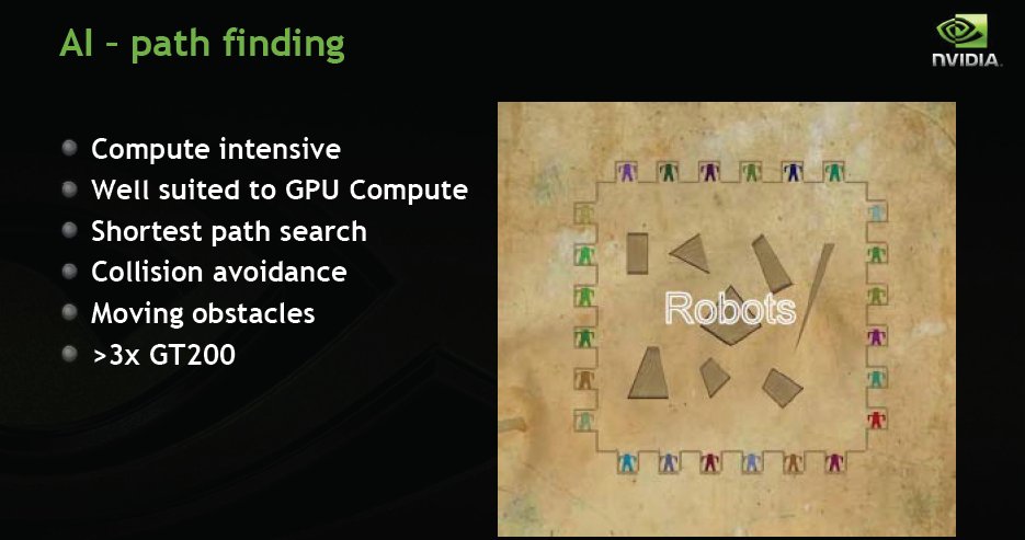
AI path finding, surely if you game you’ve seen enemy AI bouncing off obstructions in their path. It happens and we just get used to it and off the AI that’s stuck during path finding. Fermi has 3x the AI path finding capabilities of GT200 so now it’s just up to the game developers to learn better AI techniques to take advantage of that.
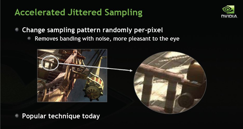
Accelerated Jitter sampling. Layman’s terms pixel pattern changing to blend in game materiel to a more pleasing (to the eye) image.
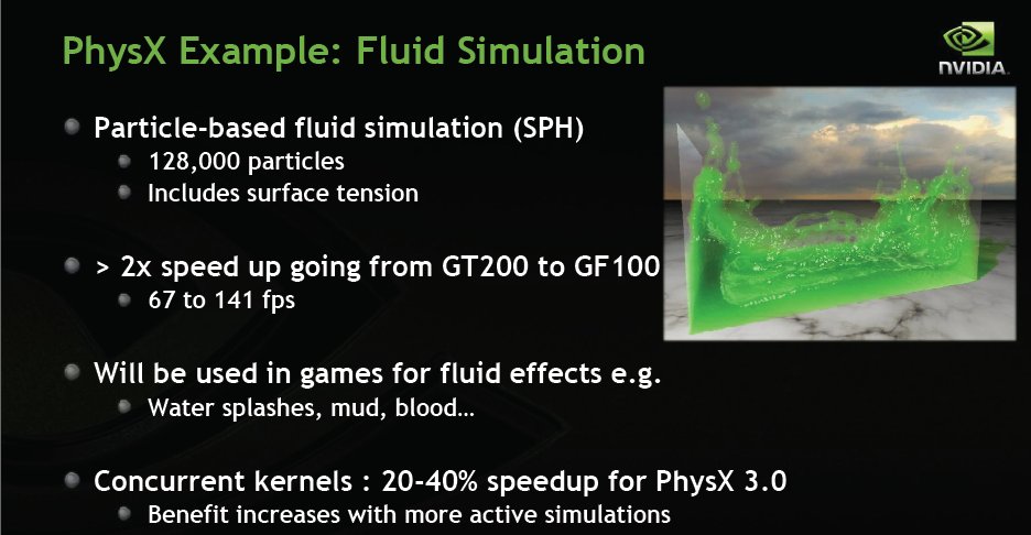
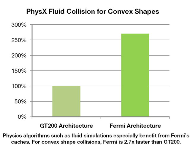
Fluid, smoke, water, shadows, and dust have always been a serious impediment in game realism. Water in general is often just a shifting shaded skin that alternates to fool the eye a little. PhysX enables the shifting of the simulation required for the computations from the CPU to the GPU and Fermi is almost twice as fast as GT200. More PhysX more realism less that doesn’t look quite right. Less that doesn’t look quite right means more realism.
PhysX is hard to explain but seeing is believing. Here’s a YouTube of a PhysX SPH Fluid Simulation. One YouTube is worth a thousand words.
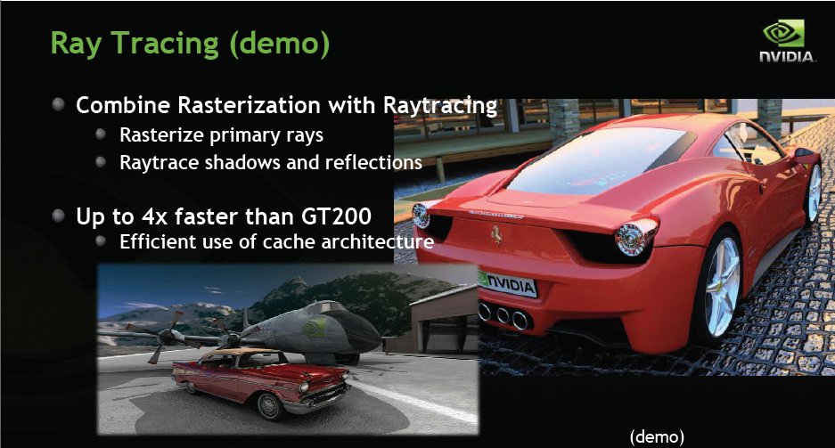
Ray Tracing and it’s persistence forces it’s inclusion in game developing. Ray tracing depending on the length of the trace (say infinity) can be very demanding so it’s used sparingly. Fermi will allow for more use of ray tracing and is up to 4x faster than GT200.
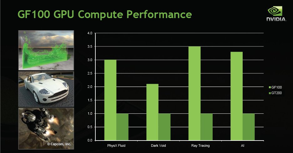
Fermi’s GPU compute performance ranges from slightly over 2x the performance of GT200 to 3.5x the performance in these tests.
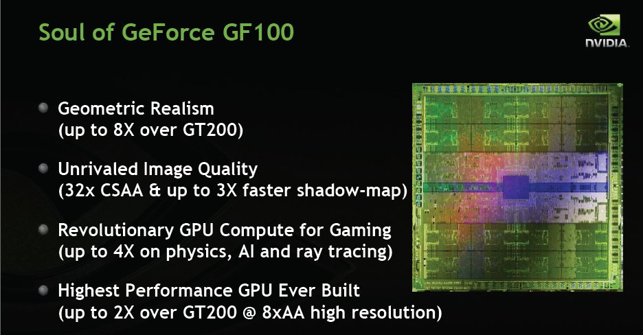
This slide pretty much speaks for itself, notice the up to 2x performance over GTX-200.
TEMPERATURES
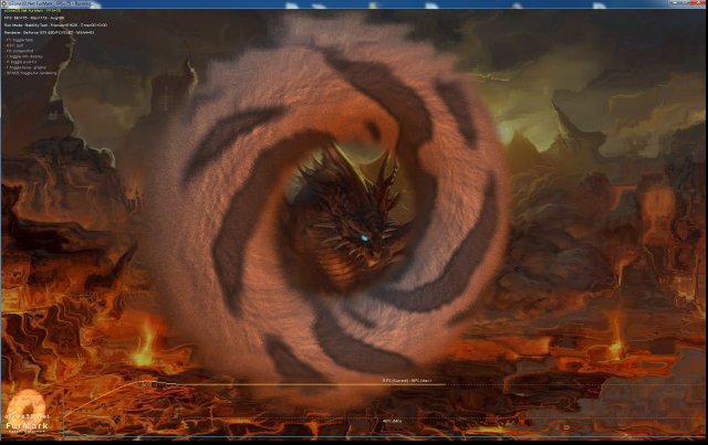
To get our temperature reading, we ran FurMark looping for 10 minutes to get the load temperature. To get the idle temp, we let the machine idle at the desktop for 30 minutes with no background tasks that would drive the temperature up. Please note that this is on an open test station, so your chassis and cooling will affect the temps your seeing.
| GPU Temperatures Auto Fan | |||
| Idle | Load | ||
| 48°C | 95°C | ||
Now that’s a little rough for temperature and we have concerns about that. Nvidia tells us that top thermal limit on the Fermi line is 105°C and we’ve seen 95°C – 96°C in Stalker COP benchmark running at 1920×1200 Ultra Setting with Tessellation enabled. We’ve seen 95°C – 96°C in Unigine Heaven 1 and 2 when the game is driving the GTX-480 at 96 – 97% core usage. We’ve verified those temperatures with another reviewer in Sweden (Thanks Bjorn) and it’s a hard and confirmed fact that Fermi is one hot GPU.
We’ve got some Furmark Screenshots we’ll show you in a few moments but lets cover 100% fan first.
| GPU Temperatures 100% Fan | |||
| Idle | Load | ||
| 30°C | 75°C | ||
Furmark was reporting 50°C starting temperature at idle with 100% fan. We dropped back to the Beta version of GPU-Z Nvidia has been helping with and read a 36°C idle temperature from there. The 75°C is from a 10 minute run in Furmark at 100% fan.
The sound from the fan while on auto is pretty minimal but in my opinion, and I have communicated this to Nvidia, the fan ramp up needs to be much more aggressive. When we hit 95°C in Furmark the fan ramped up and the temperature dropped to 91°C and remained steady there. That’s far to hot for our liking but Nvidia says thermal limits are 105°C.
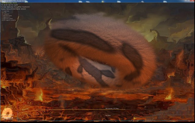
Sound from the fan at 100% was rather annoying and while we don’t measure dB it was annoying. It was pretty irritating and if I had to guess I’d say in the 65dB range. (We have since tested Fermi with a dB meter and updated the sound level, we got 65dB at 87% fan she’s a screamer!) Let’s take a look at the Furmark screenshots so there’s no doubt about measuring those blazing temperatures. The small images you can’t read but click on them for a massive image you can read.
If you take a look at this screenshot (Auto Fan) you’ll see that the temperature spiked at 96°C and the fan finally ramped up a little and the temperature leveled out at 91°C. Furmark is usually harder on temperatures than anything else but with the GTX-480 it wasn’t uncommon to see temperature rise to 96°C in Heaven and Stalker benchmarks. Believe us, we watched the thermals with baited breath and one hand on the kill switch.
We haven’t tested SLI yet but imagine two of these hot tamales sitting side by side hitting 96°C each. Nvidia recommends an extremely well vented chassis and not putting them in PCI-E slots that are right next to each other and we would assume Triple SLI is out of the question short of 3 water cooled GTX-480’s and even then chassis cooling will be paramount.
Furmark must warm up the GPU (because a 2D application is running) prior to taking readings because we read 50°C starting temperature and 76°C maximum and it fluxed between 75°C and 76°C. That is at 100% fan which we are pretty sure no human can tolerate for more than short bursts. Put it this way, the dog slinked into the other room and gave me stink eye from the noise associated with 100% fan. My better half left the room to watch TV in the bedroom. So dogs and better halves don’t appreciate the noise associated with 100% fan. Even at 100% fan the 76°C is more acceptable but having seen 95°C – 96°C in benchmarks we have serious concerns about temperatures and aftermarket cooled versions might be more acceptable.
We popped the cowling off the GTX-480 and took a couple of last minute shots so lets take a look at those real quick.
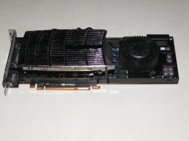
The Cooling setup extends through the plastic cowling and is exposed to the air inside the chassis making good airflow more important than ever.
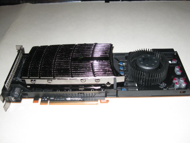
Looks to be a standard squirrel cage fan but we’ve seen it above 5000 RPM on 100% and you can imagine it’s a tad loud at that RPM (79 dB measured). Notice that the entire PCB is covered by a metal shield with some components exposed through openings. Considering the heat we’ve seen the GTX-480 generating that might be a mistake.
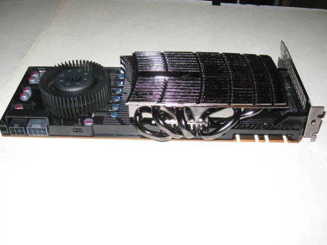
The GTX-480 gets it’s cooling capacity from 5 heatpipes and a pretty good sized heatsink with a lot of cooling vanes. Having a top exhaust like the GTX-295 had might have helped the heat buildup but we aren’t engineers so maybe they know something we don’t.
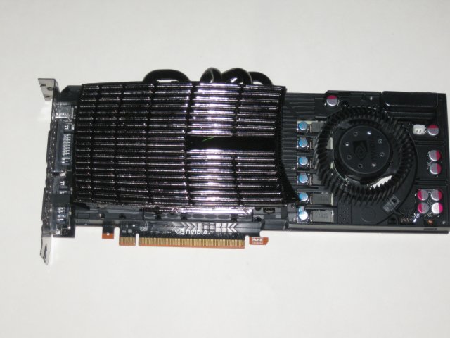
Here’s a top down shot so you can see the exposed components and the chips. Again notice the full metal shield that seems to cover most of the PCB.
Testing & Methodology
The GTX-480 is a new core design with a lot of innovative features so we are all over the map in testing. We benched the GTX-480 mercilessly for 4 days averaging 12 hours a day then started building charts and checking facts. We don’t like to do GPU reviews in that short a period and prefer a couple of weeks but we had seven days total. Given the 7 day timeframe until NDA lifted we used the Red Bull approach and more than 13 Red Bulls were killed in the writing of this review. So if you are a Red Bull hugger you are out of luck.
The first thing we did after updating the fresh load OS (From a HD clone that had no GPU drivers) was run thermal testing on the GTX-480. We were amazed that it was hitting 95° C so at that point we set our jaws and made the decision that we needed intensive benchmarking sessions lasting countless hours. We did that to simulate heavy gaming sessions and find any result that might have on the GTX-480. Often we end up benching for an hour or so and tend to other matters. Not in this case. We benched in 6 hour sessions without break. When we did have to move it was during a benchmark run.
We ran a wider variety of tests and each test was ran 3 times and the average reported here. A few tests were run many more than three times but we took the median 3 results and averages those. We’ll tell you why we ran some tests many more than 3 times a little later.
Test Rig
| Test Rig “Quadzilla” |
|
| Case Type | Top Deck Testing Station |
| CPU | Intel Core I7 965 Extreme (3.74 GHz 1.2975 Vcore) |
| Motherboard | Asus P6T6 |
| Ram | Corsair Dominator DDR3 1866 (9-9-9-24 1.65v) 6 GB Kit |
| CPU Cooler | Thermalright Ultra 120 RT (Dual 120mm Fans) |
| Hard Drives | Patriot 128 GB SSD |
| Optical | Sony DVD R/W |
| GPU Tested |
Asus 5970 |
| Case Fans | 120mm Fan cooling the mosfet CPU area |
| Docking Stations | Thermaltake VION |
| Testing PSU | Thermaltake Toughpower 1200 Watt |
| Legacy | Floppy |
| Mouse | Razer Lachesis |
| Keyboard | Razer Lycosa |
| Gaming Ear Buds |
Razer Moray |
| Speakers | Logitech Dolby 5.1 |
| Any Attempt Copy This System Configuration May Lead to Bankruptcy | |
Synthetic Benchmarks & Games
| Synthetic Benchmarks & Games | |
| 3DMark Vantage | |
| World In Conflict Benchmark | |
| Crysis v. 1.2 | |
| Dark Void PhysX Only | |
| FarCry 2 | |
| Stalker COP | |
| Crysis Warhead | |
| Unigine Heaven v.2.0 | |
| Intel DX11 SDK | |
| 3D Vision | |
| Intel DX11 SDK | |
| Nvidia Raging Rapids | |
You can see we are indeed all over the map, DX9, DX10, DX11, Tessellation, old, new and in between. We wanted as wide a representative sample as possible in the time available. We would have liked to include more and if time allows we may but in a 7 day time frame we are cutting ti down to the wire as it is.
World in Conflict Demo
World in Conflict is a real-time tactical video game developed by the Swedish video game company Massive Entertainment, and published by Sierra Entertainment for Windows PC. The game was released in September of 2007. The game is set in 1989 during the social, political, and economic collapse of the Soviet Union. However, the title postulates an alternate history scenario where the Soviet Union pursued a course of war to remain in power. World in Conflict has superb graphics, is extremely GPU intensive, and has built-in benchmarks. Sounds like benchmark material to us!
Yes World in Conflict is a little, ok a lot, long in the tooth but that’s one reason why we fall back to it occasionally. Vendors don’t expect us to bench it and we get a candid look at how the new stuff performs on what used to be a GPU crippling game.
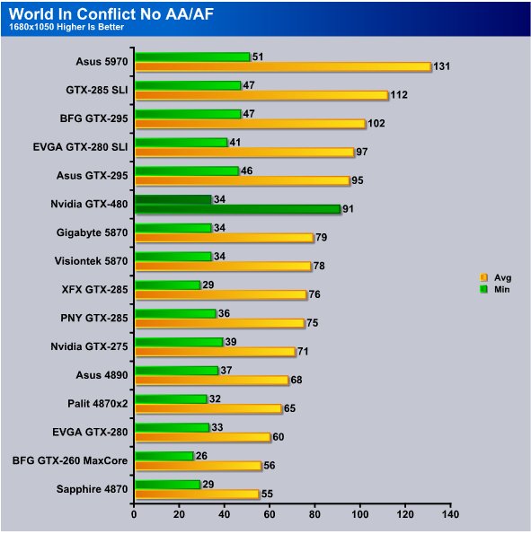
Even at 1680×1050 World in Conflict seemed a little CPU bound and we got 34 FPS min and 91 FPS average. Perhaps choosing off beat games does catch some credibility. Notice frame rates in this older game are the same for min FPS as the 5870 but the GTX-480 picks up the win on average FPS. While we have multi-GPU and dual core GPU’s on the charts we will be focusing on single core vs single core GPU’s in our review.
We may take a little criticism for focusing on single core vs single core but fact of the matter is it’s just not fair to compare multi-core GPU’s against single core.
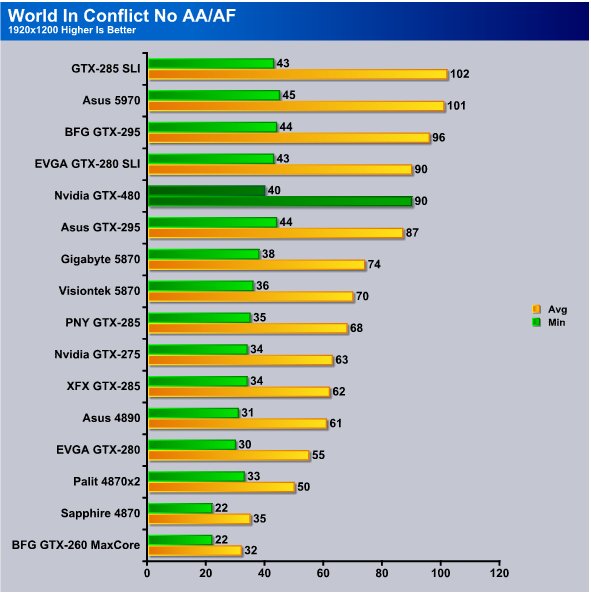
Running 1920×1200 we got 40 FPS min and 90 FPS avg and the 5870 is dragging behind by about 2 2FPS min and 16 FPS avg.
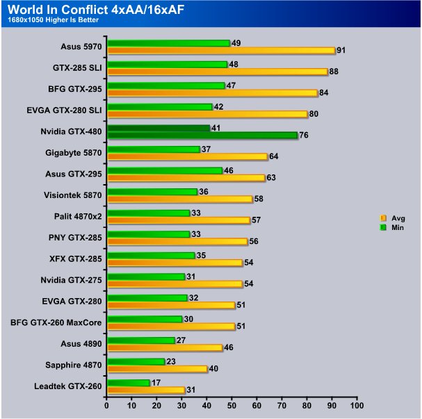
Turning AA/AF on the GTX-480 got 41 FPS min and 76 FPS avg and in minimum FPS barely tops the 5870 but in avg FPS is 19 FPS ahead of the HD5870.
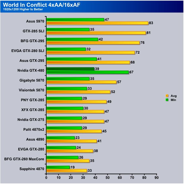
Running 1920×1200 with AA/AF enabled the GTX-480 hits 39 FPS min and 67 FPS Avg and is 6 FPS ahead of the HD5870 min and 10 FPS ahead on avg FPS.
Crysis v. 1.21
Crysis is the most highly anticipated game to hit the market in the last several years. Crysis is based on the CryENGINE™ 2 developed by Crytek. The CryENGINE™ 2 offers real time editing, bump mapping, dynamic lights, network system, integrated physics system, shaders, shadows, and a dynamic music system, just to name a few of the state-of-the-art features that are incorporated into Crysis. As one might expect with this number of features, the game is extremely demanding of system resources, especially the GPU. We expect Crysis to be a primary gaming benchmark for many years to come.
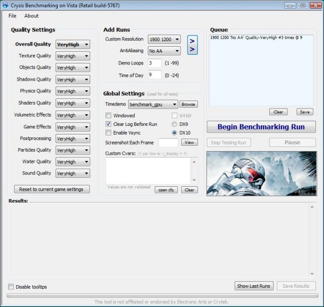
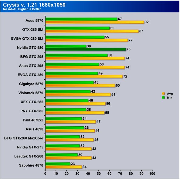
Crysis is always hard on GPU’s and it looks like at 1680×1050 the GTX-480 is struggling more with Minimum FPS than we thought it would. Performance on minimum FPS ia about that of a 4890 but the average FPS is world class.
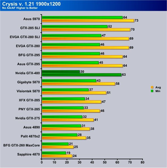
Since GTX-480 is designed to take advantage of AA/AF we are going to extend testing on it (by itself) to two different levels of AA/AF and see just how good it is. Without AA/AF minimum FPS are at 30 and average FPS are at 63.
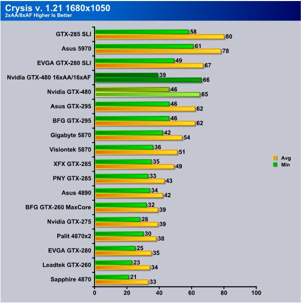
Now that’s looking better, at 2xAA we actually get higher FPS than we did at the same resolution without AA/AF. Crank it up to 16xAA/16xAF and we lose 7 FPS min but pick up 1 FPS average.
Now we may catch flak for only testing the GTX-480 at the much higher AA/AF setting and not testing the other cards at that. So be it, try receiving a new GPU, benching for 4 days straight, charting and writing a full length comprehensive review on a completely new GPU core in 7 days then complain. We will likely test the 5870 and 480 at higher AA/AF in a separate review but at this point we are looking at under 48 hours to the release time so live what we could accomplish. We aren’t really happy with it either but we don’t set the deadlines we just live with them.
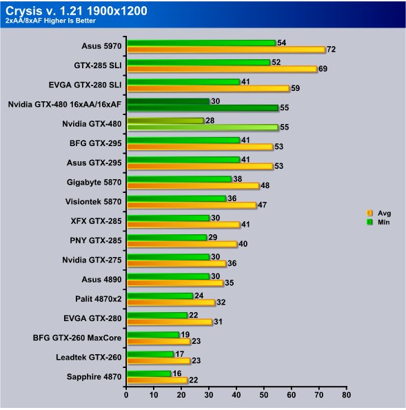
Now highest resolution tested with 2xAA we got 28 FPS Minimum but kicking the GTX-480 to 16x/16x we picked up 2 FPS on the minimum FPS and stayed at 55 FPS average. At least in Crysis it looks like the GTX-480 likes having AA/AF turned on.
Crysis Warhead
Crysis Warhead is the much anticipated sequel of Crysis, featuring an updated CryENGINE™ 2 with better optimization. It was one of the most anticipated titles of 2008.

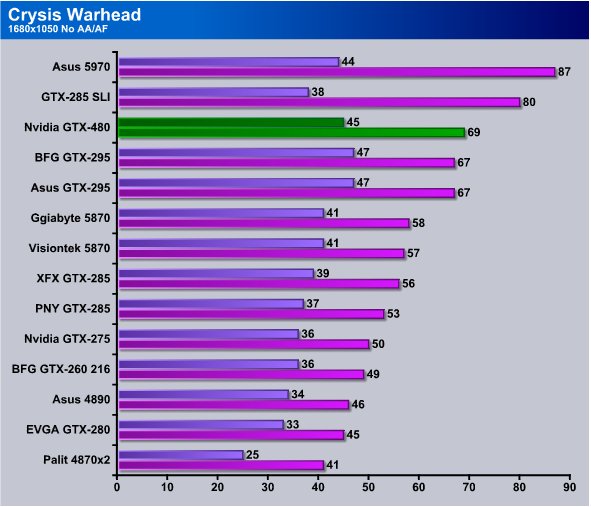
Warhead like most of the games we benched sees the GTX-480 running as fast as the GTX-295 which was our favorite dual core GPU until the HD5970 came out. Still a single core GPU running in direct comparison to a dual core GPU from the pervious generation is pretty amazing.
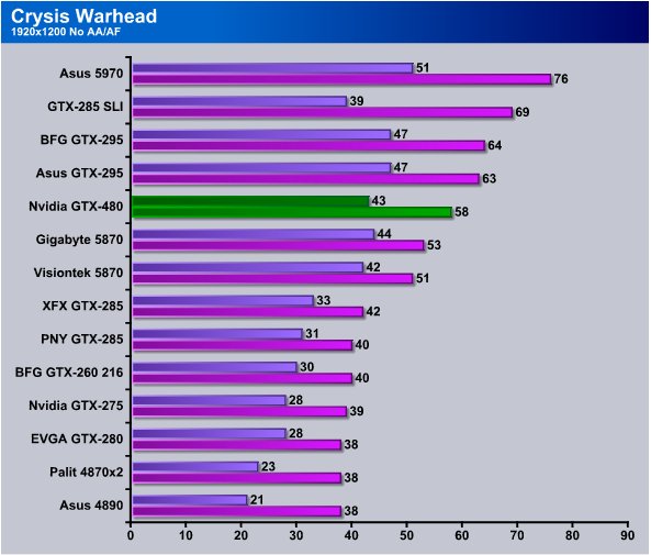
At 1920×1200 Warhead sees the GTX-480 at 43 FPS min and 58 FPS avg and the GTX-295’s pull a little out ahead but the HD 5870 is about the same on minimum FPS but the GTX-480 comes out ahead on average FPS and takes a slight win.
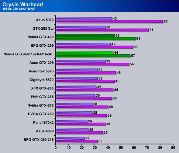
Turning AA/AF on at 1680×1050 the GTX-480 hits 45 FPS minimum which is unheard of for single core GPU’s and cranking it up to 16xAA/16xAF we dropped one mere FPS at the minimum FPS level and dropped 4 FPS on the average FPS. Dust off Crysis and run it with one of these bad boys if you really want to see what it is supposed to look like, it’s quite stunning.
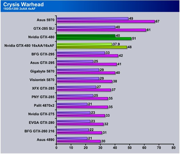
Now at 1920×1200 2xAA/4xAF knocks single core GU’s to their knees without exception, until now at least. The GTX-480 is the only single core GPU we’ve seen capable of maintaining above 30 FPS minimum. At 2xAA we got 40 FPS and averaged 51 FPS. Crank up the AA/AF and we got 37.9 FPS min and 48 average so there’s not much degradation in performance for using high AA/AF levels on Fermi. Eye candy anyone?
Far Cry 2
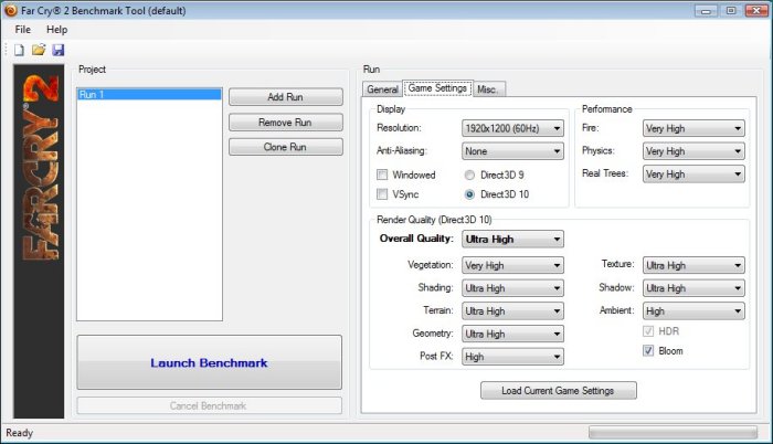
Far Cry 2, released in October 2008 by Ubisoft, was one of the most anticipated titles of the year. It’s an engaging state-of-the-art First Person Shooter set in an un-named African country. Caught between two rival factions, you’re sent to take out “The Jackal”. Far Cry2 ships with a full featured benchmark utility and it is one of the most well designed, well thought out game benchmarks we’ve ever seen. One big difference between this benchmark and others is that it leaves the game’s AI (Artificial Intelligence) running while the benchmark is being performed.
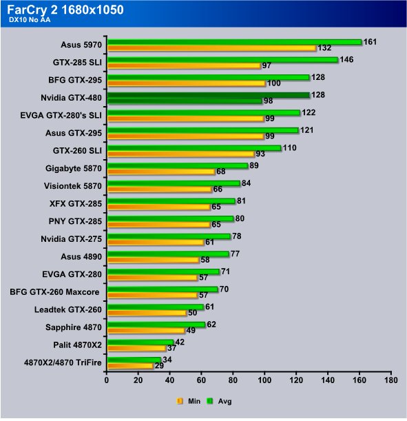
FarCry 2 at 1680×1050 isn’t very damanding to modern cards but it does scale well across GPU’s. We saw the GTX-480 at 89 FPS min and 128 FPS avg and once again it’s doing as well as the GTX-295 and much better than the HD5870.
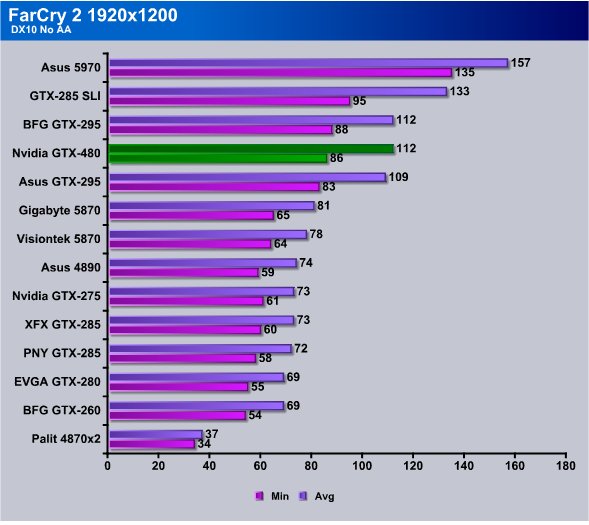
Running 1920×1200 we got 86 FPS min and 112 avg and again it’s running as fast as the GTX-295 and well above the HD5870.
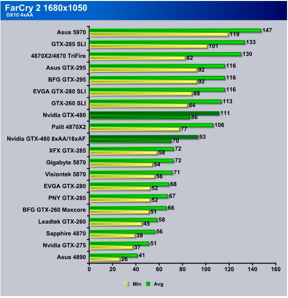
Here at 1680×1050 with AA/AF turned on we got 86 FPS min with 4xAA/8xAF and it averaged 111 FPS. Crank the AA/AF up to 8x/16x and we got 70 FPS min and 93 FPS avg. Having more than double the frame rate required to run smoothly and even wit extra AA/AF still performs above the HD 5870.
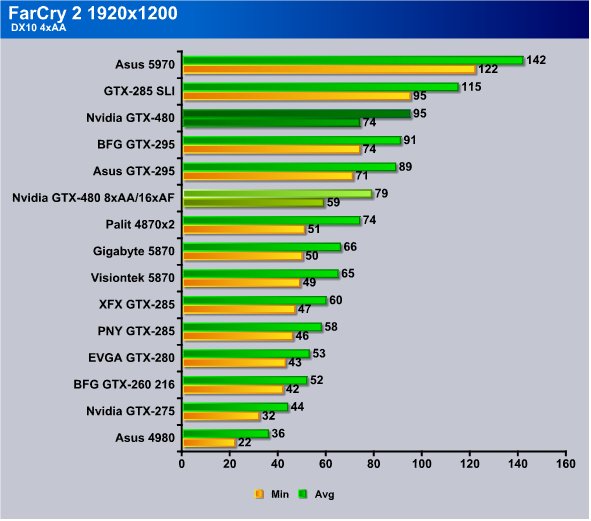
Maximum resolution tested with AA/AF we got 74 FPS min and 95 avg. Ratchet it up a notch to 8xAA/16xAF and we got 59 FPS min and 79 FPS avg. Even with the extra AA/AF we are still seeing higher performance from the GTX-480 then the HD5870 which was running at 4xAA/8xAF. We will have to get into more high AA/AF testing later but GTX-480 is looking like it eats AA/AF for breakfast.
S.T.A.L.K.E.R.: Call of Pripyat
Call of Pripyat is the latest addition to the S.T.A.L.K.E.R. franchise. S.T.A.L.K.E.R. has long been considered the thinking man’s shooter, because it gives the player many different ways of completing the objectives. The game includes new advanced DirectX 11 effects as well as the continuation of the story from the previous games.
Since we now have both Nvidia and ATI DirectX 11 cards to compare against each other you can expect a lot more attention to be paid to DX11 benches and games. Tessellation and God Rays (AKA Sun Shafts and other Ray Tracing effects) will also be part of our re-focus.
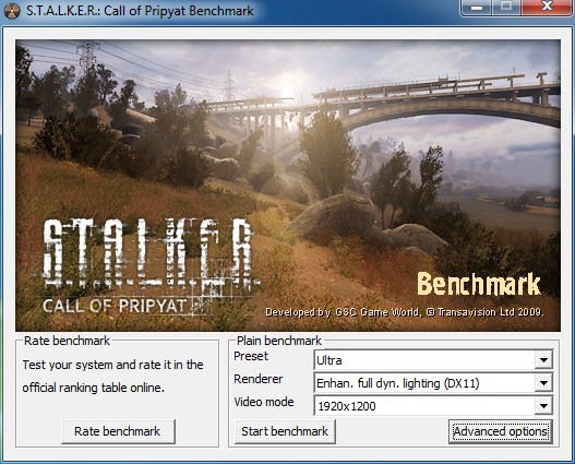

GTX-480, Fermi (GF100), is geared for Ray Tracing and while Nvidia has told us that current technology won’t support real time fully Ray traced objects in games aren’t possible introducing it in small doses is. GTX-480 is 2.5 times more efficient than GTX-285 is at Ray Tracing but even that quantum leap in capabilities isn’t enough to expect massive Ray Tracing to be feasible in games.
The GTX-480 hit an amazing 87.35 FPS average in Stalker COP with God Rays included in the scoring. How we did this was run Stalker 3 times, add all the FPS together and divide by the total number of tests. Four tests per run, three runs, add all the FPS and divide by 12. It’s the same as adding all four scores from Stalker together and dividing by 4 except we make three runs at it and divide by 12.
Notice that the GTX-480 suddenly jumps ahead of the HD5890. The Single largest reason for that is Fermi’s enhanced Ray Tracing capabilities. This ability and the results let’s you see the inherent power of Fermi and part of the direction Nvidia is betting gaming will take.
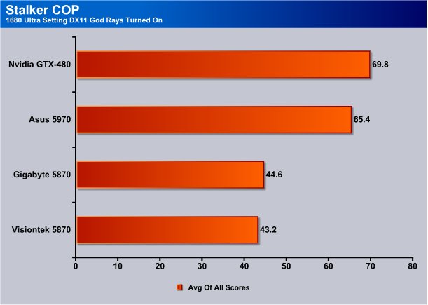
Here again we see GTX-480 topping the dual core HD5970 but HD5970 narrowed the gap a little.
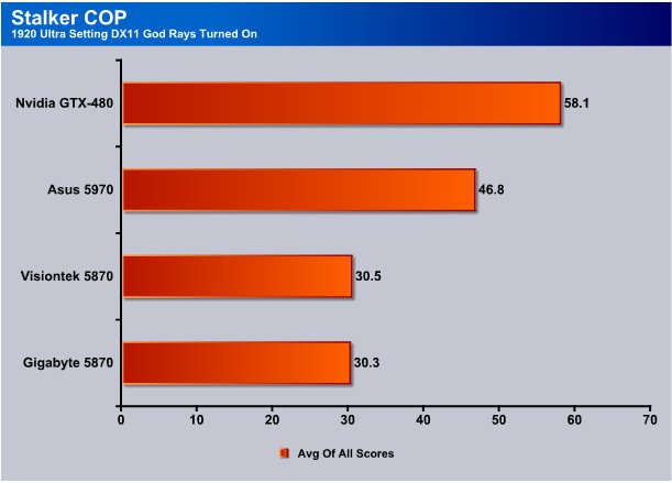
Top resolution tested GTX-480 hits 58.1 FPS averaged and it’s about 11 FPS faster than the HD5970. Notice that the HD5870 is running at 30(Ish) FPS and Fermi is running almost twice as fast.
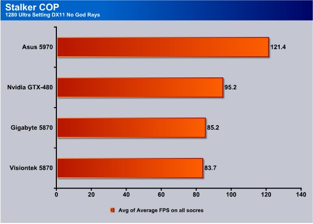
Now let’s take God Rays out of the equation. To do that we took the same scores but excluded the God Rays and used 3 scores from each run, three runs total and divided by 9.
Take Ray Tracing out of the equation and the HD5970 jumps back out into the lead. The GTX-480 is still topping the HD5870.

Here again we see the HD5890 on top without God Rays in the equation. Turn God Rays on and the situation is quickly reversed. Looking at the HD5870 performance is good but the GTX-480 still tops it.
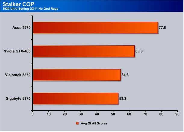
Top resolution tested the GTX-480 easily outpaces the HD5870 and the HD5970 still sets on top the pile without God Rays in the equation.
What this should be telling you is that in games and applications that are capable of Ray Tracing on the GPU the GTX-480 is king. If Gaming uses Ray Tracing heavily Nvidia’s design bet will pay off in spades.
3DMark Vantage
For complete information on 3DMark Vantage Please follow this Link:
www.futuremark.com/benchmarks/3dmarkvantage/features/
The newest video benchmark from the gang at Futuremark. This utility is still a synthetic benchmark, but one that more closely reflects real world gaming performance. While it is not a perfect replacement for actual game benchmarks, it has its uses. We tested our cards at the ‘Performance’ setting.

The GTX-480 scored a 17417 on the GPU portion of 3DMark Vantage and as far as Vantage is concerned barely ahead of the HD5870. The The HD5870 score you see here had the advantage of an overclocked CPU and the GTX-480 was stock speed so for what it’s worth the GTX-480 might have scored a little higher with the same CPU OC. What you should take from the chart is that as far as Vantage is concerned the GPU score doesn’t go up with a CPU overclock which is why we report the GPU score and not the total score.
Unigine Heaven 2.0
Unigine Heaven
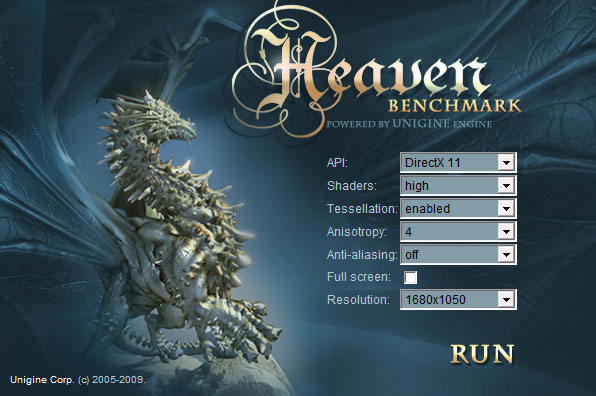
Unigine Heaven is a benchmark program based on Unigine Corp’s latest engine, Unigine. The engine features DirectX 11, Hardware tessellation, DirectCompute, and Shader Model 5.0. All of these new technologies combined with the ability to run each card through the same exact test means this benchmark should be in our arsenal for a long time.
The settings we used in Unigine Heaven
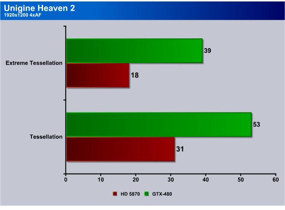
In Uningine Heaven 2 we got 39 FPS at 1920×1200 4xAA with Extreme Tessellation turned on, the HD 5870 got 18 FPS which would be unplayable frame rates. Regular Tessellation the HD5870 got 31 FPS and the GTX-480 got 53 FPS. So DirectX11 with Tessellation and AA/AF is going to be a booger on GPU’s but he eye candy is really nice.
Dark Void
We were only interested in PhysX in Dark Void so we only ran the GTX-285 and GTX-480 to get a peek at generational differences between Nvidia GPU’s. PhysX will run on the CPU when you have an ATI GPU installed and that’s not a fair comparison so we didn’t go there.

Dark Void shows the GTX-285 hitting 48 FPS at 1680 and the GTX-480 is hitting 105 FPS so we are seeing more than twice the performance. We are getting the same results at 1920 and the GTX-480 hits 94 FPS and the GTX-285 hits 43 FPS. Generationally speaking the GTX-480 is performing more than 2x faster than the GTX-285 and we’ve seen up to 2.5x performance in PhysX.
Microsoft DirectX 11 SDK
The Microsoft DirectX 11 SDK package gives us a platform (Nvidia or ATI) independent method of testing Tessellation. Since Microsoft’s DirectX standard has to run on both Nvidia and ATI GPU’s equally well and if there is any noticeable difference it’s in hardware or driver implementation on the GPU vendors end.
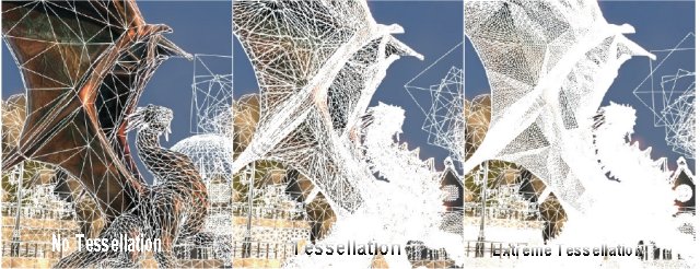
Please note that this image isn’t from Microsoft DirectX 11 SDK. This shot just shows you the basics of Tessellation . The first image is just a stock image without Tessellation. The Second image is Tessellated and the third image is Extreme Tessellation. Tessellation takes a geometrically flawed image that shows spiked edges because of the triangles used and smooths it down by adding a ton more triangles.
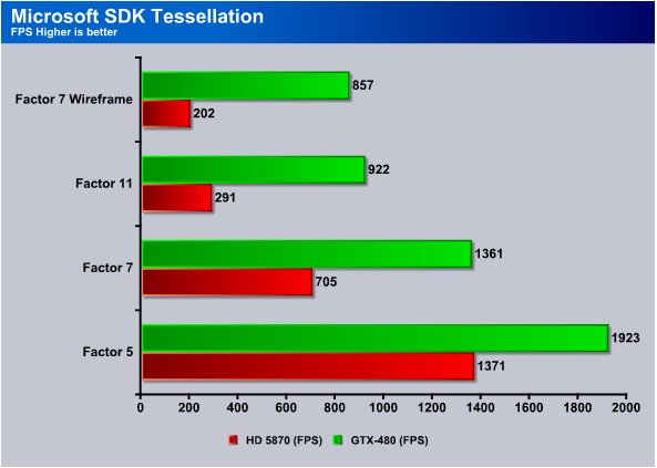
This test consists of a Tesselated wireframe and several different factors of Tessellations. In the Factor 7 Wireframe the GTX-480 hit 857 FPS and the HD5870 only cranked out 200. While that may look like a lot of FPS it’s actually a measurement of how each GPU performs. The GTX-480 performed 4x better in this test.
The Factor 11 test sees the GTX-480 hitting 922 FPS and the HD5870 hitting 291 so figure about 3x performance on the GTX-480.
The Factor 7 test shows 1361 FPS on the GTX-480 and 705 on the HD5870 and the HD5870 is narrowing the gap as less Tessellation is used.
Factor 5 sees the HD5870 at 1371 FPS and the GTX-480 at 1923 FPS so we are getting a good picture of how much more effective the GTX-480 is at Tessellation than the HD5870.
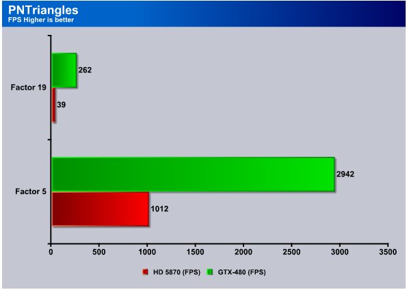
We decided to crank it way up on PNTriangles and the GTX-480 was up to the task. It churned out 262 FPS and the HD 5870 only managed 39 FPS. Drop that down to Factor 5 and the GTX-480 cranked 2942 FPS and the HD5870 churned out 1012 FPS.
Now let’s get something straight. Tessellation is usually scalable, so there may be in game adjustments for the level of Tessellation. The game may automatically scale Tessellation. So no one will be left out but some will be left with less eye candy and the rough edged graphics we see today. Now I’m ok with carrying my 2 year old cell phone but graphics I want EYE CANDY so sweet it makes the eye ache.
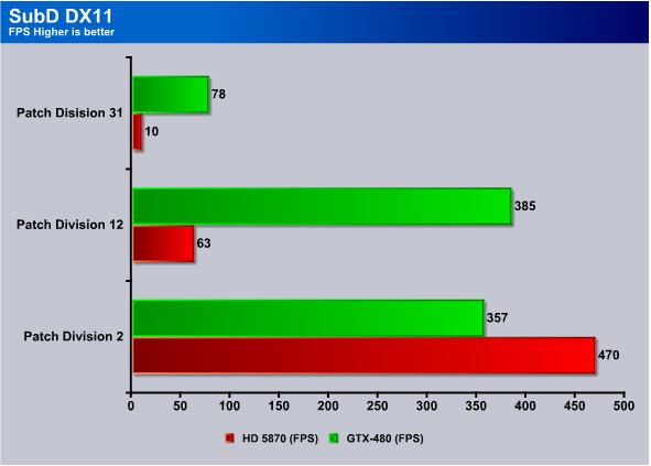
We know you have to be asking yourself what the heck is SubD. SubD is Tessellation of Displaced Subdivision surfaces. DX11 allows for displacement mapping. If you read through the review you should know what displacement mapping is. It’s the raising of mapped surfaces to show depth or height. Think of the DX11 spikes on the Dragon in the Unigine benchmark.
At patch division 31 the GTX-480 pushes 78 FPS while the HD5870 drops to 10 FPS. Move to Patch D. 12 and the GTX-480 hits 385 FPS while the HD5870 hits 63. Lower patch division to it’s lowest setting and the HD5870 outperforms the GTX-480 but set that low the game developers probably wouldn’t even use it.
3DVision
Since the introduction of 3DVision we’ve been on top games in 3D and performance in 3D might not interest every end user but it interests us. The gaming in 3D is fantastic and it’s so immersive that until you’ve tried it you can’t understand how much it adds to gaming.
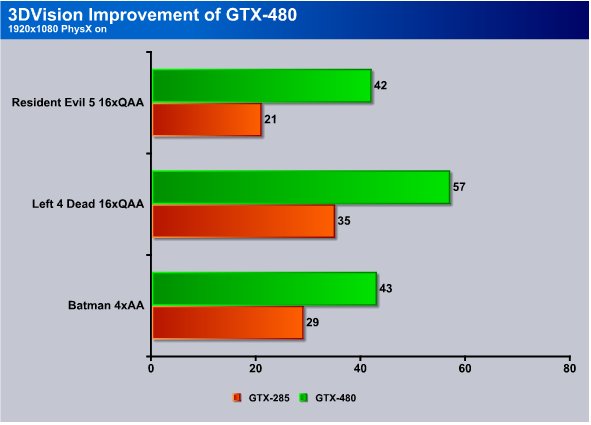
We ran three different games in 3D and measured the performance of each game on both GPU’s.
In Resident Evil 5 at 16xQAA the GTX-480 blazes in at 42 FPS while the GTX-385 only manages 21 FPS in this GU crushing game.
In Left 4 Dead the GTX-285 managed 35 FPS and the GTX-480 hit 57 FPS and 3DVision improvements on Fermi are looking good.
In Batman at 4xAA we got 29 FPS from the GTX-285 and 43 FPS from the GTX-480. Keep in mind that in 3DVision each frame has to be rendered twice for each eye and it can drag down performance. You give up FPS but beyond 30 FPS graphics are rock solid to the eye. You lose FPS but you gain the 3D ex[erience.
OVERCLOCKING
Lets take a look at a GPU-Z shot of the Nvidia GTX-480 before we get into the overclocking problem.
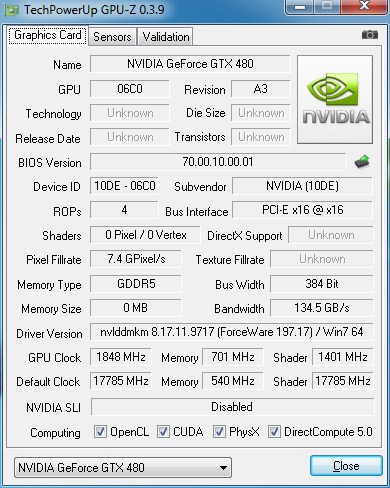
To begin our GTX-480 journey we had to deal with GPU-Z seriously reading the new card wrong. We’ll explain “wrong” with the next screenshot.
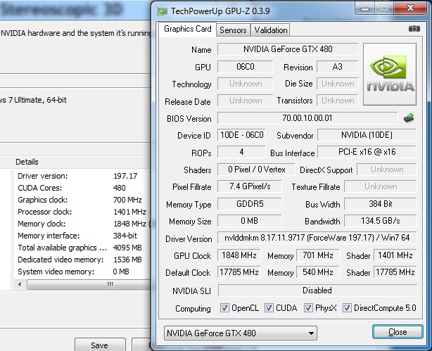
Notice that in this shot Nvidia control panel is reporting the Core Clock correctly, but GPU-Z reads Graphic clock as memory but at double speed. It reads the Memory clock as the GPU Core. The overclocking utilities read it the same way.
We have a beta of GPU-Z that reads the card correctly.
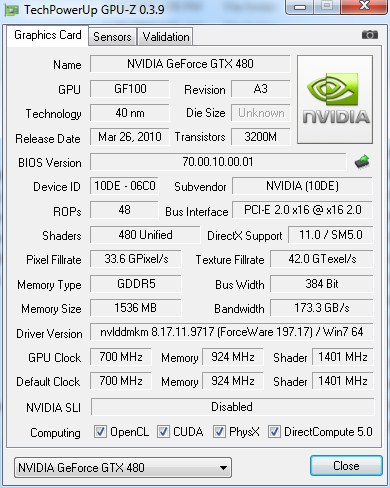
Here’s the GPU-Z beta with the correct specifications. Imagine OCing a 96c capable card with faulty or iffy OCing utilities. We’ll wait until the OCing utilities catch up a little and revisit Fermi.
Conclusion
Well we are afraid time beat us this round. We have other content we would like to post but it will have to take the form of a tack on to the review. Still left untouched due to time constraints, StoneGiant DX11 Benchmark, 3D Surround and 3DVision Surround, CUDA and a few games. We beat the GTX-480 for about 72 hours in a six day time frame and we are impressed with it both in performance and endurance.
The 3 Billion transistors stuffed on the 480 cores really churn out the eye candy and the newly restructured core is more efficient at Tessellation and Ray Tracing than anything we’ve seen to date. Performance remained high no matter what we threw at the GTX-480 and the only potential problem we have seen with it so far is heat. It responds very very well to ultra high AA/AF levels and we saw games looking like nothing we’ve ever seen. Crysis was absolutely beautiful at high AA/AF and frames were flying by,
You stuff 3 Billion transistors on a 40nm process and 1.5 GB of ram and all the feature this chip packs you can expect some heat. We saw thermals running as high as 95°C in Furmark, Stalker and Heaven. Nvidia assures us that the GPU is fine up to 105°C but we expect aftermarket air and water cooling to be popular on the GTX-480. Figure the power of the GTX-295 dual core GPU packed into a single core GPU and toss on half a ton of new features the GTX-295 never dreamed of. One small note while in the throws of benchmarking fatigue I accidentally pulled the GPU out of the rig while it was still hot and got a 1st degree burn. It’s that hot so be careful and make sure your chassis is well ventilated and if running SLI separate the cards by one PCI-E slot. Planning on Triple SLI plan on water cooling.
Fermi represents a quantum leap in GPU graphics and computing. It’s a little bit of a bet on games embracing Tessellation and Ray Tracing but Nvidia hedged their bet by equaling the performance of the GTX-295 without the new technologies factoring in. Play a game with Tessellation and/or Ray Tracing and performance is more than double.
We like what GTX-480 represents, which is what Nvidia is taking a notice of what developers and end users want, and we are sure every vendor does. Nvidia seems to go that extra step and not only notice what end users want but goes beyond that and sends teams to help implement the technology. Optimizes code on games to run faster, produces a GPU the scientific community can embrace and use as relatively low cost supercomputers. Provides the toolboxes developers need to use the technology and takes a bottom up view of their role in GPU production.
It’s an old concept but one often forgotten in business today. Look at what the end users want and give them more than that. Once you have the product the end user wants, make it easy for him to use. Nvidia has excelled at that and provides the team to help implement and teach the developers how to use the tools they have given them.
Getting back to the GTX-480 it’s massively powerful and we expect it to be some time before developers catch up to the copious bounty Nvidia has provided with the GTX-480 and Fermi lineup. Expect them available at your local E-Tailor on April 12th, 2010 and the MSRP is $499 for the GTX-480 and expected to be $350 for the GTX-470. Nvidia assures us that there are tens of thousands of GPU’s available for retail sale at launch so we shouldn’t see much if any bottleneck on supply to demand.
Being late to market with a DirectX 11 GPU may hurt them a little and price points and market saturation with DirectX 11 capable GPU’s at lower price points should be a priority for Nvidia. With two flagship GPU’s hitting shelves in April we would like to see a 460 model at a lower price point but still in the enthusiast class. Then we’d like to see some mainstream offerings with Fermi’s design at lower price points. With GT200 it wasn’t as important to push mid-range cards because they weren’t saturating the market with DX11. Now that Nvidia is DX11 capable we would expect them to want to saturate every price point with DX11 capable cards and spread the joy that is Fermi as widely as possible.
| Nvidia GTX-480 | ||||||||||||||||||
|
||||||||||||||||||
|
Summary: The Nvidia GTX-480 brings a lot to the table and the feast it lays out is succulent. With 480 exposed cores, double the previous generations cores, 15 streaming processors, 60 texture units, 1.5GB of GDDR5 and a 384 bit memory bus the GTX-480 extrudes mind blowing raw power. Backing up all that muscle is a half ton of new features previous generations of Nvidia GPU’s can only dream about. The 40nm manufacturing process placing 3 Billion transistor at Fermi’s command is a formidable engineering feat. Then give Fermi what it needs for Ultra AA/AF, Ray Tracing, and Tessellation this is one eye candy feast you shouldn’t pass up. We could say more about the GTX-480 but our 3DVision glasses have recharged and the next 6 or 7 hours we are going to play Crysis the way it was meant to be played.
|
 Bjorn3D.com Bjorn3d.com – Satisfying Your Daily Tech Cravings Since 1996
