
We still have to wait a couple of months until Kaveri—the successor to the Trinity APU—is released. However, AMD is ready to talk a little bit about the upcoming APU. While we do not have any specific information on the model and the clockspeed, we have a bit of information regarding one key feature in Kaveri: the heterogenous Uniform Memory Access or hUMA.
AMD first integrated the GPU onto the CPU with their Fusion platform. The original Fusion processor—Zacate—was designed for low power computing devices. Its primary target was to compete against the Intel Atom processor that is powering many netbook. The desktop version APU was released with the introduction of the Llano in 2011. Last year, we saw the successor to Llano with the Trinity. And later this year, we are expecting to see the successor to Trinity.
AMD has been refining its APU performance by improving the parallelism and the interconnection between the different components inside the APU. With Llano, AMD integrated the CPU and the GPU on the same die. Trinity improves the CPU performance with Piledriver, over the K10 found on the Llano. Trinity also allows the GPU to access the system memory through translation service and page fault management.
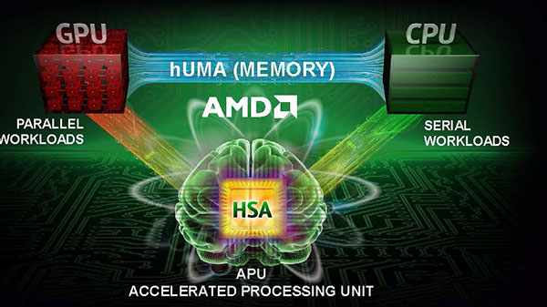
With the next generation APU (Kaveri), we should see improvements on both CPU and the GPU front through the architectural change (Steamroller for CPU and the GNC for the GPU). In addition, Kaveri also unified the memory address space where both CPU and GPU can access the memory into the same address space. AMD called this heterogenous Unified Memory Address or hUMA.
As you may recall, AMD is one of the founders for the Heterogeneous System Architecture (HSA) whose goal is to build a “heterogeneous compute ecosystem, rooted in industry standards, for combining scalar processing on the CPU with parallel processing on the GPU while enabling high bandwidth access to memory and high application performance at low power consumption.” hUMA is the first step from AMD towards achieving such a goal.
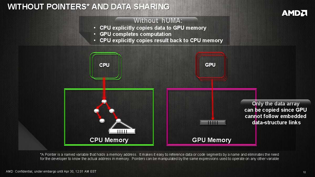
All of the current APUs and CPUs use UMA or NUMA to handle the memory between CPU and the GPU. If a task is assigned to the GPU, the CPU must first explicitly copied data to the GPU memory. Then the GPU can access the data to complete the computation. The result then is copied back to the CPU memory.
This is a rather inefficient way of doing things as data needs to copied back and forth before each component can access it.

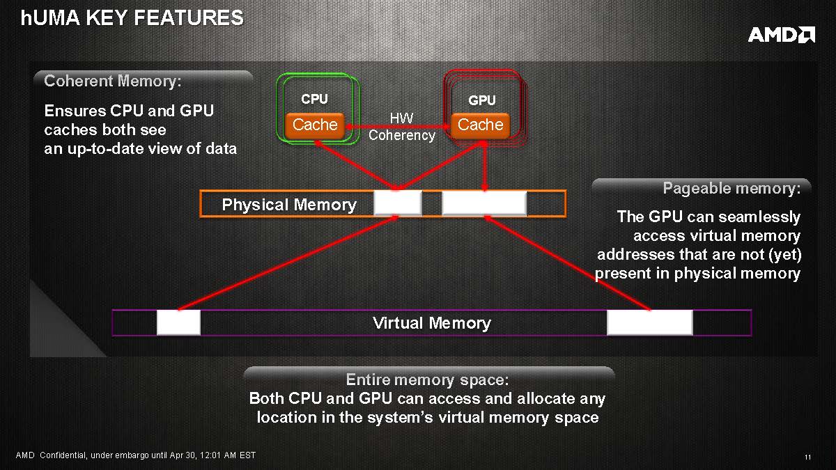
With hUMA, all processing cores (CPU and GPU, etc) share single memory address and operates at the same bandwidth. CPU and GPU caches both see the data stored in the memory and can access and allocate any location in the system’s virtual memory. Data no longer needs to be copied back and forth between the CPU and the GPU before they can be seen. The CPU can pass a pointer and its entire data structure to the GPU. The result from the GPU can be read directly by the CPU without the need to copy.

hUMA brings the following features:
- Access to entire memory space
- Pageable memory
- Bi-directional coherency
- Fast GPU access to system memory
- Dynamic memory allocation
Not only can the CPU and GPU can both access the same memory address space, the new structure also maintains cache coherency at the hardware level. The GPU now can access and cache data from coherent memory region of the system memory and reference the data from the CPU cache. This allows a finer grained data sharing between CPU and the GPU.
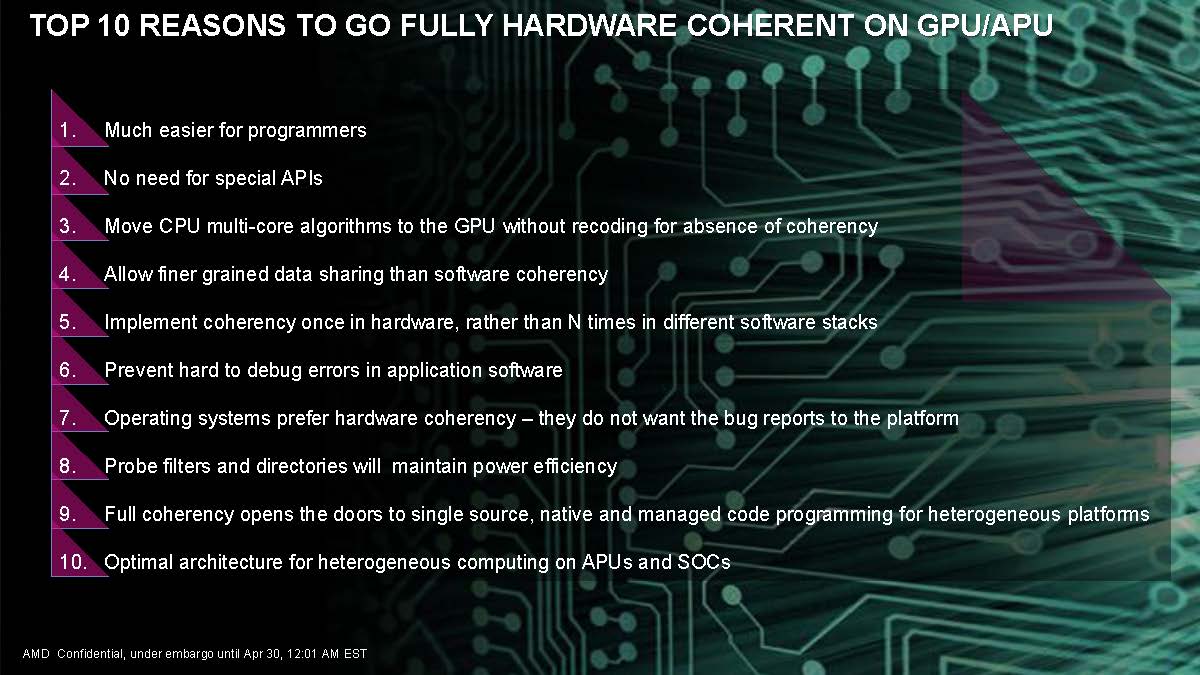
The immediate obvious benefit with hUMA would be the elimination of the extra step in copying the data so the GPU would have a faster access to the system memory. This would mean that a task can be completed in less time.
Additionally, there is also a power efficiency implication as well. Since GPUs are better at floating point calculations than CPUs, if a code can take the advantage of the GPU computing power that is inside the APU more efficiently, it would be able finish the task quicker and would spend more time at idle, which would reduce the power consumption. AMD’s estimates that the GPU can do greater floating point calculation at a quarter of power consumption compared to the CPU. With everything moving toward mobile platforms, this means longer battery life.
For programmers, hUMA would mean much easier programming since they do not need to code their software to specifically use GPU for computing.Programmers also do not need to maintain two different sets of codes, since hUMA supports mainstream programming languages such as Python, C++, and Java. It would also make it much easier to debug code. It would also let programmers to port their existing code to the GPU much easier.
Given the fact that the GPU on the AMD APU has a clear advantage over what Intel offers on their CPUs, it is no surprise that AMD wants to put a greater emphasis on the GPU computing power. With hUMA, AMD is hoping to gain greater support from the software engineers to port or write applications to fully utilize the highly parallelized GPU cores. We think the HAS and hUMA is moving AMD (and the industry) towards the right direction where we can better utilize the various computing powers (CPU, GPU, or even ARM) that is available for maximum efficiency. Assuming that AMD can gain enough support, Kaveri and any future APUs from AMD would put AMD in a very good position at offering excellent performance by leveraging various architectures and resources at its disposal.