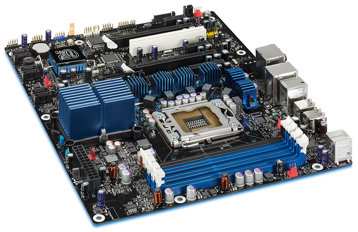
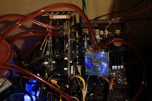
Every once in a while Intel, comes out with a phenomenal performing motherboard with a chipset and CPU to match. We going to look at such a product, the Smackover X58 Motherboard.
INTRODUCTION
For the last six months or so, we all have been awaiting the arrival of a highly anticipated motherboard from Intel. We’ve all heard the rumors and we’ve seen all the sneek peeks, but it just wasn’t enough for us. We wanted MORE. I bring you one of those most highly anticipated products from Intel, the Smackover motherboard. This motherboard is being armed with Intel’s latest chipset, the X58 northbridge, and it was paired up with an already proven southbridge, the ICH10R. The X58 northbridge chipset has the capability of cross platforming GPU’s from ATI’s Crossfire to NVIDIA’s SLi all on the same board. Fully supporting tri-channel DDR3 memory, using three sticks of memory instead of two sticks of memory, for even more memory bandwidth. The X58 chipset, supports up to 36 PCI-Express 2.0 lanes, so it is possible to have two PCIe x16 slots and one PCIe x4 slot on the same motherboard.
The performance of the Smackover motherboard is simply put, “Mind Blowing”. Overclocking the Core i7 CPU with this motherboard is very easy compared to the Core 2 CPU’s. I better get on with the review before I get too carried away. I know, too late.
About Intel
Intel pushes the boundaries of innovation so our work can make people’s lives more exciting, fulfilling, and manageable. And our work never stops. We never stop looking for the next leap ahead—in technology, education, culture, manufacturing, and social responsibility. And we never stop striving to deliver solutions with greater benefits for everyone.
Technology Leadership
It began with the Intel® microprocessor, the invention that sparked a revolution. Intel’s history of developing groundbreaking technology continues today. We attract the most brilliant minds in science to push the boundaries of innovation and further our position as the world’s leader in semiconductor technology. Our passion is to create technology that changes the world.
Corporate Responsibility
Intel is driven to create bold advancements in technology that enhance people’s lives. Explore how Intel is cultivating the spirit of innovation and promoting the concept of sustainability in our operations and in communities worldwide.
Company Information
At Intel, we believe in being open to big ideas and inspired innovation that will change the world. This idea of openness is at the very core of who we are as a company. Stay connected to the latest news and opportunities from Intel, and learn more about our values and vision for the company.
SPECIFICATIONS
| Test Setup &Testing Methodology | |
| Form factor | ATX (12.00 inches by 9.60 inches [304.80 millimeters by 243.84 millimeters]) |
| Processor | Support for a Intel® Core™ i7 processor in an LGA1366 socket |
| Memory | Four 240-pin DDR3 SDRAM Dual Inline Memory Module (DIMM) sockets, Support for DDR3 1600 MHzς, DDR3 1333 MHzς, DDR3 1066 MHz, Support for up to 8 GBς of system memory |
| Chipset | Intel® X58 Express Chipset |
| Audio | Intel® High Definition Audio subsystem in the following configuration, 8-channel (7.1) Dolby Home Theater* Audio subsystem with five analog audio outputs and two S/PDIF digital audio outputs (coaxial and optical) using the Sigmatel* 9274D audio codec |
| Video | ATI CrossFire* multi-GPU platform support ATI CrossFire technology enables two ATI* graphics cards to work together for ultimate 3D gaming performance and visual quality, Full support of next-generation ATI CrossFire* |
| LAN support | Gigabit (10/100/1000 Mbits/sec) LAN subsystem |
| Peripheral interfaces | Twelve USB 2.0 ports (8 external ports, 2 internal headers), Six Serial ATA 3.0 Gb/s ports, including 2 eSATA port with RAID support supplied by a Marvell* controller, Two IEEE-1394a ports (1 external port, 1 internal header), Consumer IR receiver and emitter (via internal headers) |
| Expansion capabilities | One PCI Conventional* bus add-in card connectors (SMBus routed to PCI Conventional bus add-in card connector), One primary PCI Express* 2.0 x16 (electrical x16) bus add-in card connector, One secondary PCI Express 2.0 x16 (electrical x16) bus add-in card connector, One PCI Express* 1.0a x16 (electrical x4) bus add-in card connector |
MOTHERBOARD LAYOUT
Let’s start with the usual motherboard layout first.
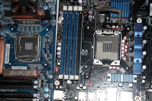
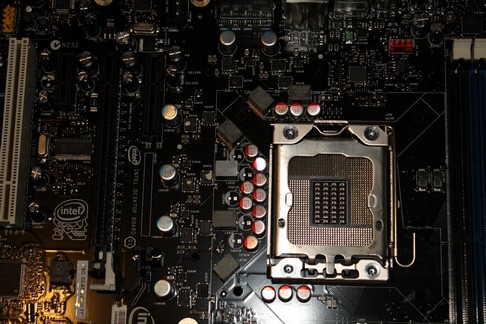
Starting off on what the differences are between the older socket 775 (Abit IX38 Quad GT left) vs the socket 1366 (Intel Smackover X58 right). Here we see Intel has not only increased the amount of pins but the actual size of the CPU socket, as well as how Intel has changed the way the pins lay down, going from one direction to two different directions.
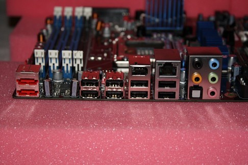
Now let’s move on to the rear I/O ports themselves. Starting form the left and working right, we notice right off the bat Intel did not include any PS2 ports. For those who haven’t already moved over to a USB keyboard or mouse, you’d better do so now if you’re considering the Intel Smackover. In the place where the PS2 ports are supposed to be, Intel has added two E-Sata ports. Moving to the right, we see Intel included 8 USB ports, and over the last 4 USB ports Intel has put a 1394 port (firewire), for those still using this interface, and 1 Gigabit Ethernet port. Right next to these are the connectors for the 7.1 audio.
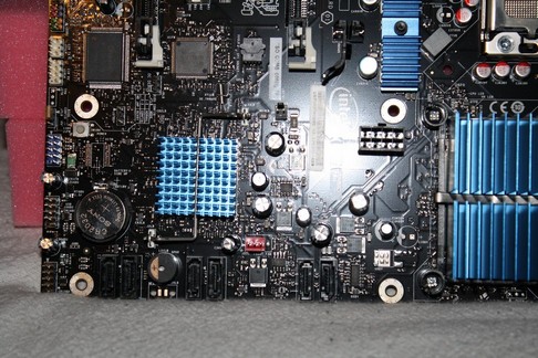
Now, let’s go over the actual board itself. At first glance of the motherboard, we can not help but to scratch our heads at how Intel laid this board out and we have to wonder what it is that they were on, because I want some of that stuff. Starting at the southbridge, which is a ICH10R, and looking to the left of the southbridge, we see an odd button. This is the power button used to power up the Smackover X58. There’s no reset button, just a power button. To the left of the power button we see that Intel has included an old style jumper for clearing the CMOS. Going down from the CMOS jumper, we have an extra 1394 front I/O connector, plus Intel has placed two more USB headers for the front of the chassis or for the for the rear of the chassis, giving us a grand total of 12 USB ports.
Moving to the right of the USB ports we see the CMOS battery. Moving straight down from the CMOS battery to the bottom edge of the motherboard we see 6 Sata 3GBs ports. Why Intel did not use a 180 degree sata ports is beyond me. In between sata ports 0, 1 and 2, 3 we see fan header #1.
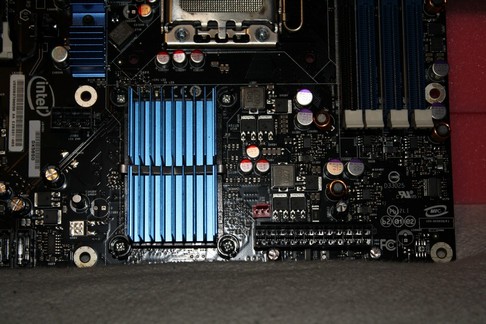
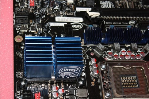
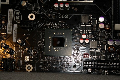
We’re moving over the northbridge (or better known as the IOH now). To the top left corner of the northbridge, we see the 8-pin EPS plug that will power the CPU and northbridge. To the right of the northbridge, we see fan header #2 and the 24-pin power plug.
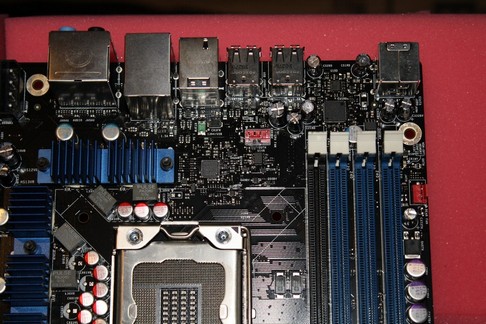
Moving up towards the CPU socket area, and to its immediate right, we see four DDR3 memory slots. Notice here that three are blue and one is black. For tri-channel memory you need to put the memory in the three blue memory slots. Right next to the memory slots on the edge of the motherboard, we see fan header #3. Moving left now, we see fan header #4 and a heatsink that helps cool the power modules that power the CPU. To the upper left corner of the picture we see a 4-pin Molex that will need to be plugged in. Right next to the Molex plug there-s a 1x PCI-E port (not shown).
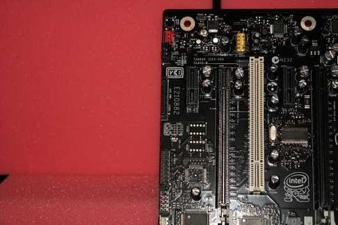
Moving to the left of the motherboard, we see that Intel used 2 PCI-E 16x ports for our video cards. In between each of these PCI-E ports Intel put a PCI slot and a PCI-E 1x. To the left of the PCI-E x16 port Intel included one last PCI-E 1x port. Right on the edge of the motherboard we see what appears to be a SATA power connector. Well, quess what it is and it also needs to be hooked up?
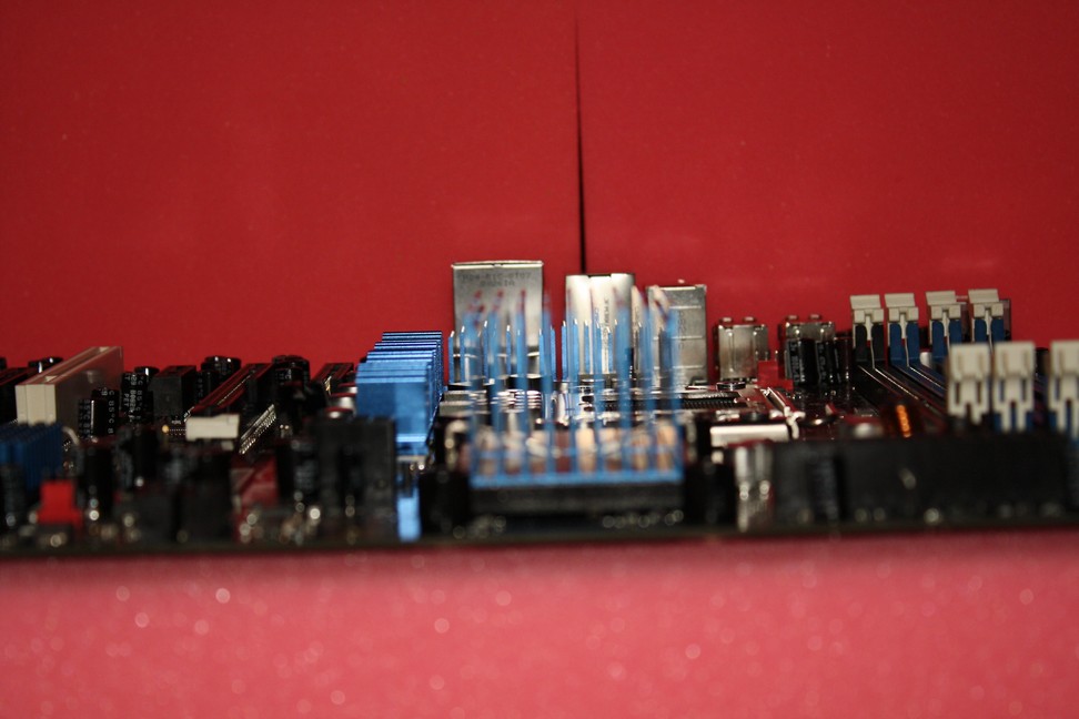
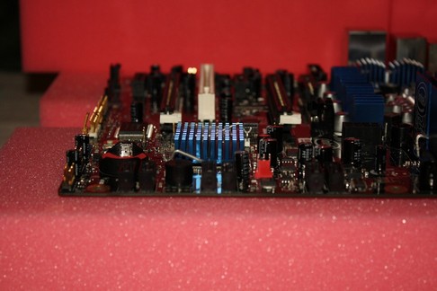
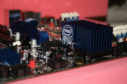
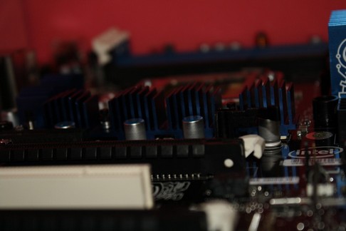
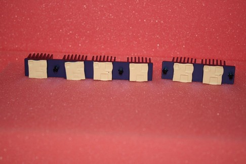
These next few images are me just taking pictures of the motherboard’s heatsinks and such to give you a better idea on how it looks.
|
|
|
|
|
|
|
|
|
|
|
|
|
|
|
|
|
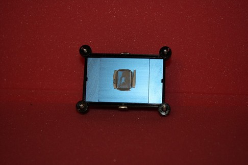
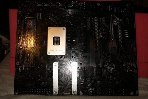
On the backside of the motherboard, we see that Intel decided to use a retention plate that serves two purposes, one to hold on to the CPU hold down mechanism for the CPU socket, and two it helps to keep the board from getting warped when using CPU coolers. Personally, I think Intel should have also made it cover the four bolt holes as well. Also, notice on the northbridge area that Intel used two metal bars to help keep the board from getting bowed here. Good job Intel.
INSTALLATION
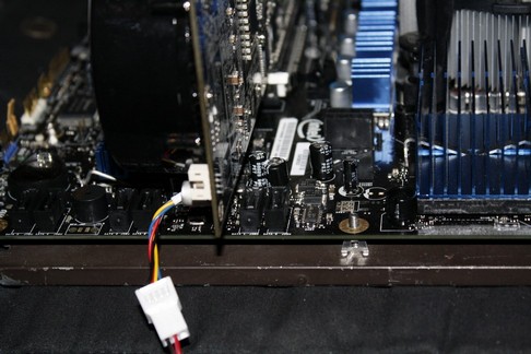
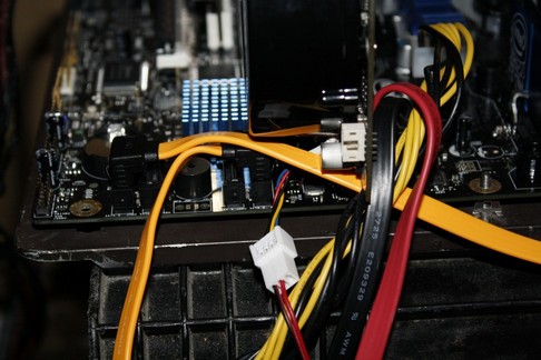
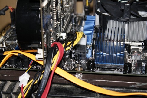
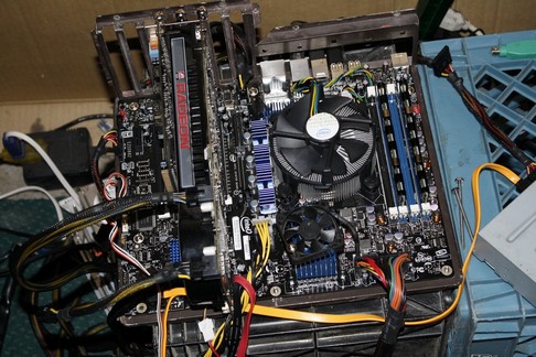
This is when I had gotten all of the components installed on to the Smackover X58 motherboard. We are looking at the right hand side of the video card (right behind it) and SATA ports 0, 1. Notice how close these are to the video card. Having such a close proximity to the video card like this will make removing the SATA cables a challange with out first removing the video card, that is, if your SATA cables have the little metal locking device.
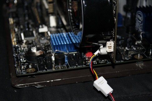
Looing at the left side of the video card we again notice that one of the two SATA cables (SATA ports 2, 3) is right below the heatsink of the video card, eliminating the use of any type of Sata cable that is not a 90 degree cable. Looking at the final set of SATA ports, SATA ports 4 and 5, we see that if we use a second video card, we will have the same issue that we had as with the second SATA ports.
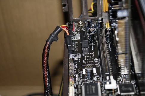
Now looking at the 4-pin Molex power plug, we can see that it’s not in an unusual place. You may want to use an Molex extension to make plugging in to this port a little easier. Now I wonder where my extension cable wondered off to. Oh well, I will just use the PSU plug for now.
Here’s how I had to hook up my SATA cables. Notice the clearance between the SATA cables and the video card. By having to use a 90 degree SATA cable, I eliminated any possiblity of using more than 4 SATA devices. If Intel used 180 degree SATA ports here, it would have made getting to these ports easier.
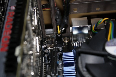
Looking at the first set of SATA ports (SATA 0, 1), we again see how close the cables are to my video card. They are actually hitting the back of it. The location of the EPS 8-pin CPU and northbridge power plug is a good placement, if you ask me. It is in a good place that can be easily reached, making sure the power plug won’t get in the way of the CPU heatsinks or any other components on the motherboard.
|
|
|
|
|
|
THE BIOS PART 1
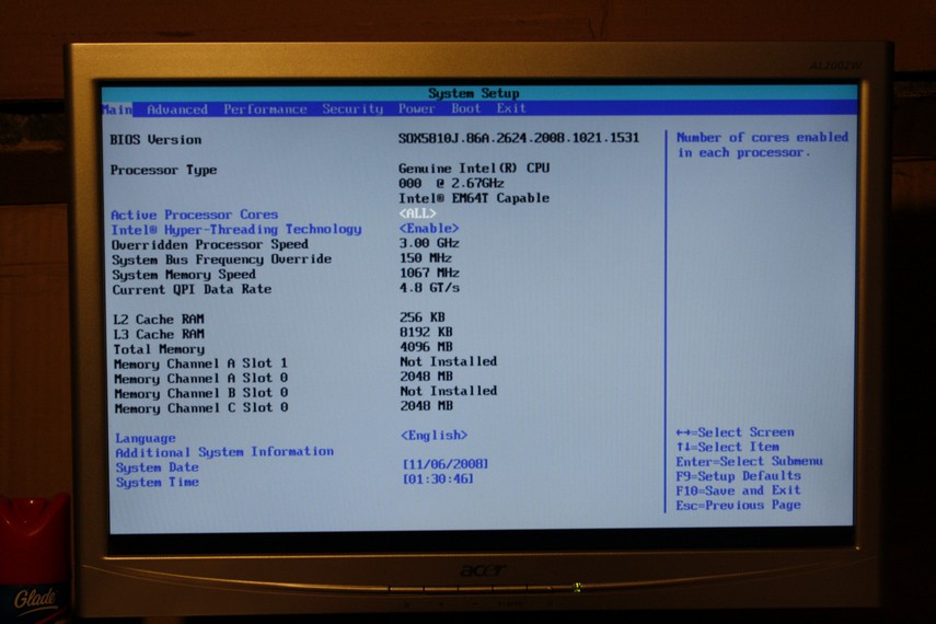
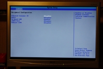
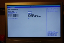
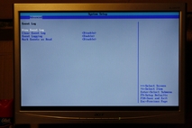
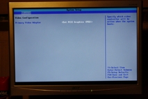
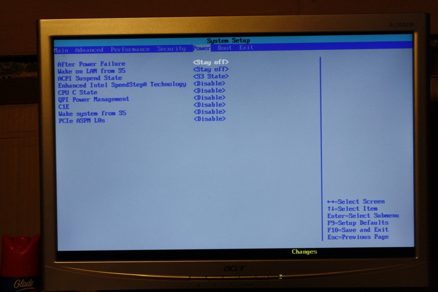
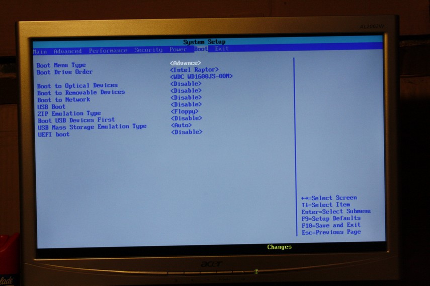
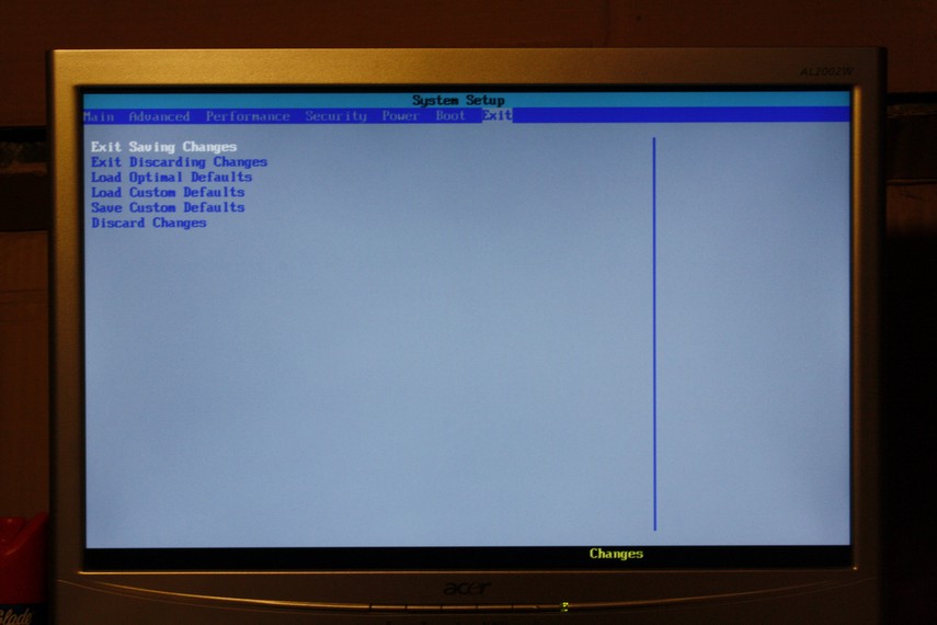
This is what the BIOS looks like. I want to mention a few things before I continue on with the BIOS. I won’t be going into great detail of the BIOS itself. All I am going to do is a hit an miss of it to give you an idea what to expect from this motherboard BIOS. To move about the BIOS you will need to the hit nter key to get into the sub menu’s and ESC to go back one page.
The BIOS kinda looks like what OEM manufacturers ( HP, Dell) use in their BIOS’s as far as the layout goes. It is fairly easy to figure out where each adjustment is at, and also pretty easy to make those adjustments. During my time spent in the BIOS, I did notice that it was somewhat sluggish going from one screen to the next, kinda like navigating through Windows in safe mode.
The main BIOS screen this will give you important information about the memory divider being used, CPU speed, and total amount of memory in use. You can turn off Intel’s Hyper threading and also turn on or off cores on the CPU itself.
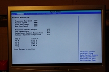
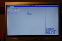
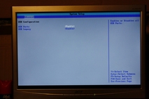
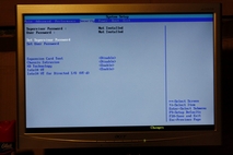
Advanced BIOS screen. This is where we can make the adjustments that we need to make, anywhere from our boot configurations (to using RAID or Normal SATA mode’s) to setting up the USB. It also will display the temperatures of our system components as well.
|
|
THE BIOS PART 2
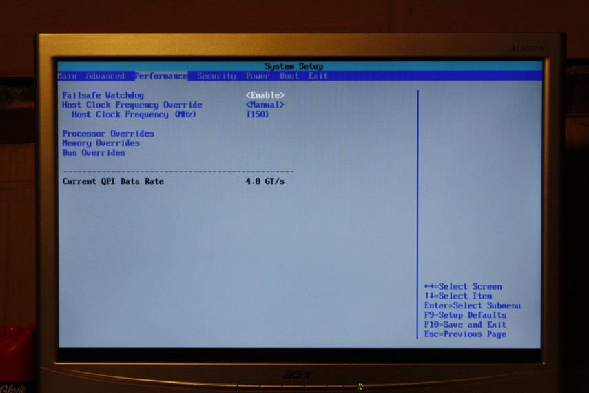
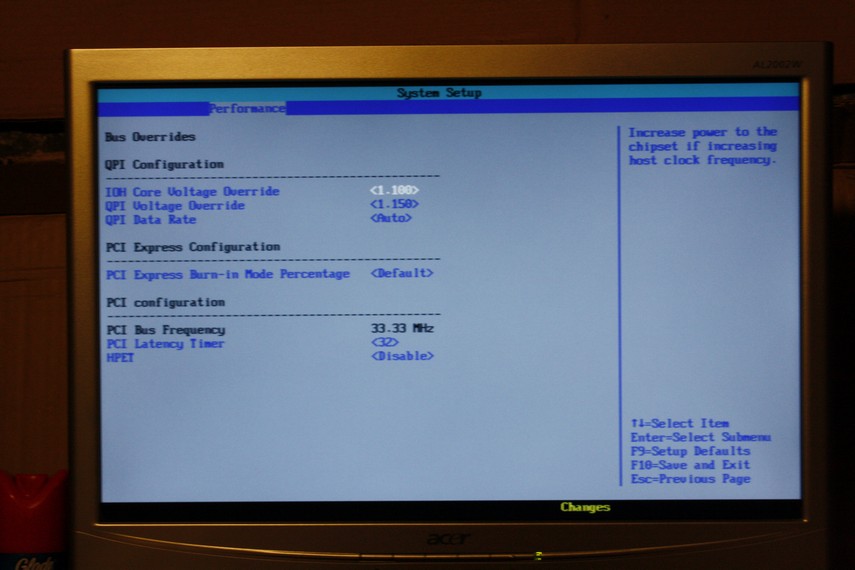
Ok, you are probably thinking, “He just skipped a BIOS screen.” To answer this question, “Nope, I didn’t. I did that deliberately”. This portion is on the performance page, that I skipped over on the previous page. This is where we make all our adjustments to our CPU and memory and the voltages for the QPI (Quick Path Interconnect), or the IOH (northbridge). Again, to move about the BIOS you will need to hit Enter to get into the sub menus and ESC to go back one page.
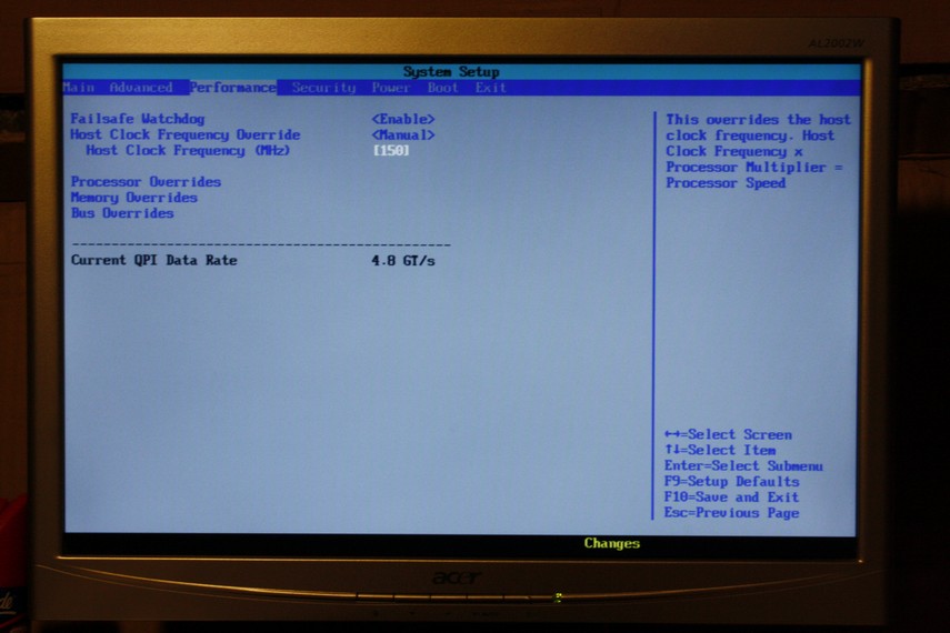
When we first see the Performance tab open up, we will see a Host watch dog setting, the Host Clock Frequency setting, The FSB adjustment, and our three primary adjustments we will be neediing to adjust our CPU, Memory, and the bus voltages. In order to Overclock the CPU we will need to set the Host Clock setting to enable. The Host watch dog setting will allow the BIOS to recover from a bad overclock, so it’s best to leave this enabled.
The FSB is named the Host Clock Frequency and by adjusting this setting you will increase the CPU frequency as well. The same rule applies here as with any overclocking endevours, CPU multi X FSB = actual CPU speed. When adjusting the FSB you cannot just type in a set frequency, you have to hit the Enter button and then use the + and – keys to move it up or down. After you set the FSB to your desired frequency you have to hit the Enter button again. If you did not hit the Enter button it would revert back to the last known FSB you had prior to adjusting the FSB, which will get annoying after a few tries.
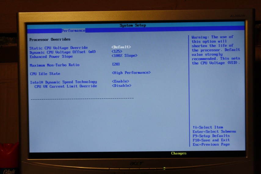
The Processor Override page is where we can adjust the CPU’s Multiplier and its voltages, and also the CPU’S Idle Mode. I set mine to High Performance so it uses the Multiplier I set it at (maximum non turbo ratio.). This is the same way as the FSB adjustment. You have to hit Enter to enter the adjustment stage, but this time you need to use the arrow keys and when you’ve reached your desired setting, you have to hit Enter again. You can adjust the CPU voltage by either using a set voltage, or by using the overvoltage option. Intel reccomends you use the overvoltage options, and so do I, as this will give you a more refined control over the CPU voltage.
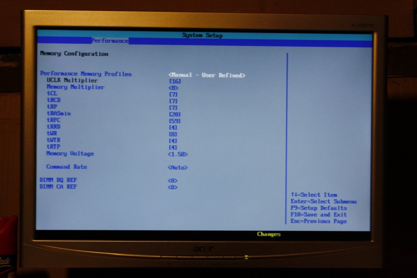
Memory Configuration page is where can adjust the Divider of the memory (options 8, 6 only, multiply this by the FSB and you will have effective memory speed) and also the timings of the memory and the voltage of the memory. Intel recomends that you DO NOT GO above 1.65 volts on the memory or you could possibly damage your CPU. The same thing go when making these adjustments as you do with the FSB, hit Enter, use the + and – keys, hit Enter when finished.
Finally the Bus Overrides page is where we can make voltage adjustments to the IOH (northbridge) to the QPI (Quick Path Interconnect),and a few otherminor tweaks reguarding the QPI burst rate and the PCI latency. Same thing making these adjustment’s as you do with the memory, hit Enter, use the + and – keys, hit Enter when finished.
This portion of the BIOS was somewhat cumbersome. Having to hit Enter and then either the + or – keys or the up or down buttons then hit Enter again to set the adjustments you made everytime and to every adjustment that was made got a little tiresome, especially if you forgot to hit enter to set that adjustement. Having to re-do the whole thing over again is a pain, especially since the BIOS has somewhat of a lag issue..
TESTING METHODOLOGY
| Test Setup &Testing Methodology | |
| CPU | Core i7 920 |
| Motherboard | Intel Smackover X58 |
| Case | Open Bench Testing Case |
| Memory | Crucial DDR3 1333 MHz |
| Video Card | Sapphire 4870×2 |
| Hard Drives | 3 x 160 Gig Sata2 Western Digital, 2 in raid 0, 1 back up |
| Cdrom Drive | Lite On Sata1 Dvd Burner |
| Power Supply | Coolermaster U.C.P. 900watt 80+ Silver |
| Type Of Coolers Used | DD MC-TDX , Koolance VID-487X2 (Dual Loop) |
| CPU Speeds Used | 2.66GHz, 3.3GHz, 3.8GHz |
| Operating System Used | Microsoft Windows Vista 64 bit Ultimate |
| Type of Software Used During Testing | Everest, CinBench, SiSoft, wPrime, Super PI, WinRar, 3DMark06, 3DMark Vanatge, Crysis, Far Cry 2 |
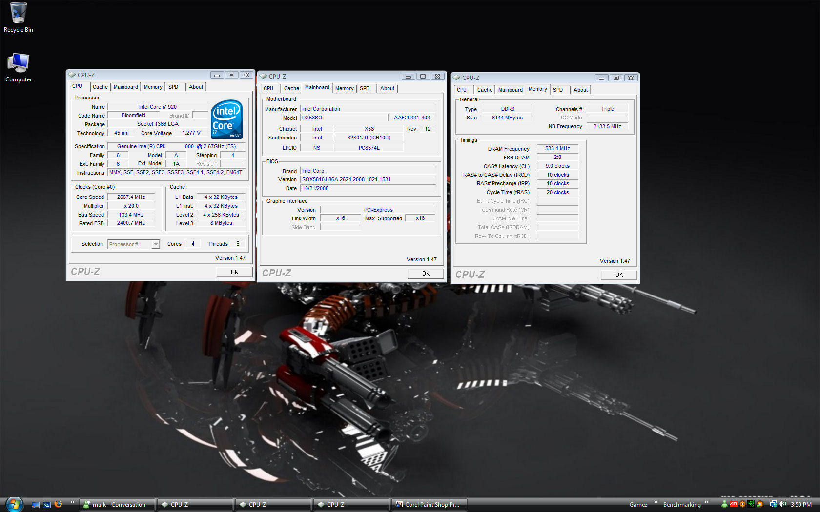
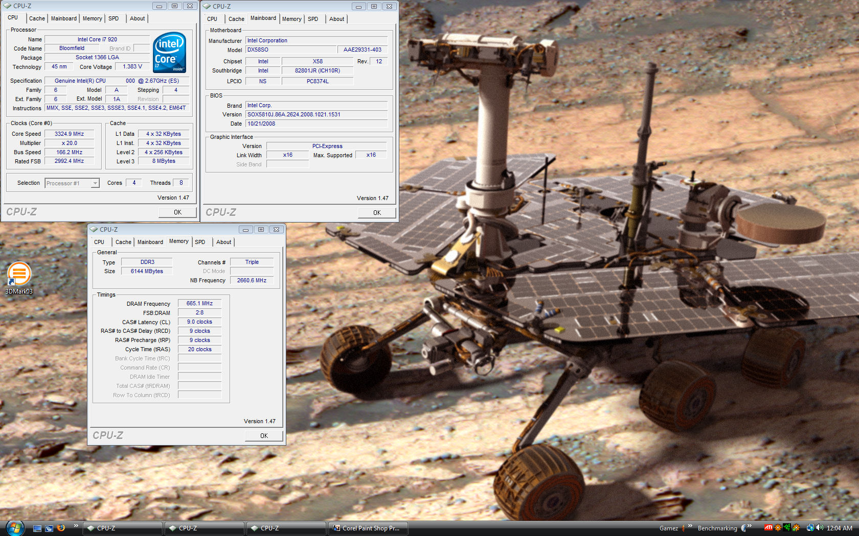
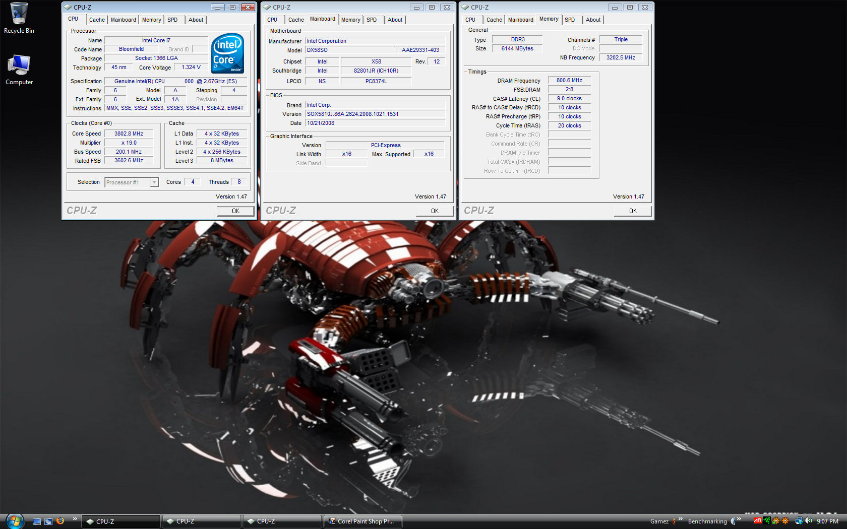
For testing purpose’s, I used three sets of FSB setting’s (along with that the CPU was overclocked). I used the bottom end of each overclocked settings of Low, Medium, and High (or extreme) settings. My low overclock was the original CPU speed of 2.66GHz (133×20), the Medium overclock was 3.3GHz (166×20), and my High overclock is 3.8GHz (19×200). I ran each benchmark two times to verify times and consistancy with my scores and also I ran these consecutively to ensure stability was present per CPU clock speed. The memory I used was Cruical 1333 9-10-10-20 at 3 x 2024 megs, totaling roughly 6 gigs of memory. I left the memory at its default timings and just increased the FSB and dropped the CPU multiplier from 20 to 19. To better show you the Smackover X58 overclocking abilities and the scaling it provides when overlcocking the CPU and memory. The memory divider I left it at 8 (2:8 or a 1:4 ratio). The only other adjustments I made were to the IOH, the QPI and, of course, the CPU voltages. The memory voltage remained at 1.62 volts and did not increase or decrease during testing. I will be comparing the Smackover X58 and the Intel Core i7 920 CPU to a Q6600 CPU at 4GHz on a GigaByte P45 Extreme with Mushkin 1600 7-7-7-20 DDR3 memory. Also, I should mention that I used a Danger Den MC-TDX water block to ensure my CPU would not overheat during testing. So, your results will vary on a case to case basis and will not mimic my results or scores.
No motherboards or computer components were harmed during testing, just slightly bruised, HAHA!!! On to the overclocking results.
OVERCLOCKING RESULTS
Overclocking the Smackover X58 motherboard was actually easy. It’s bbout the same as we did with the Core 2 Duo/Quad CPU’s. Just up the FSB, apply voltages when needed, and viola, overclocked CPU. No HyperThreading multipliers, goofy memory dividers, or multitude of irrelivant voltages and settings. I did, however, have to up the QPI voltage from its base of 1.1 volts to 1.25 volts to help stabilize the system when reaching the FSB mark of 200. The IOH (northbridge) also had to be upped from 1.0 to 1.3 volts because of artifacting with the 4870×2 I was getting during graphical testing. The one thing I learned real quick when dealing with ATI cards they like to have high PCI-E volts when overclocking the CPU. Being that this motherboard lacked any PCI-E voltage adjustments, I ended up having to use the IOH to accommodate this loss, as the northbridge (IOH) controls the PCI-E exclusively. After upping the IOH voltage, I no longer had any graphical errors or anomolies during testing.
My final FSB’s and CPU clock speeds, that I used for testing were:
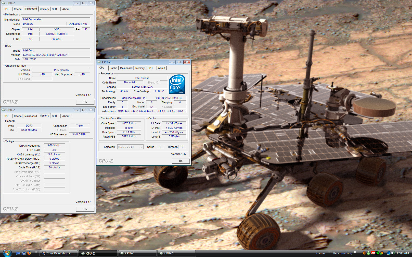
I did have some slight issues when trying to get this motherboard to go above the 200 FSB mark at first, but since I had a bit more time on the Smackover X58 motherboard, I had been able to reach 215 x 19, giving me a 4080 CPU core speed and 1720 memory speed with timings of 9-9-9-20. I was not able use this speed during the testing phase as I was having difficulty of getting this CPU frequency stable at the time of writing this review. But, nonetheless, I will still show a screen shot of it.
CPU-Z Screen Shots
SiSoft
SiSoft has always been at the forefront of the technology arena, being among the first providers of benchmarks that show the power of emerging new technologies like multi-core, GPGPU, AMD64/EM64T/x64, IA64, NUMA, SMT (Hyper-Threading), SMP (multi-threading), AVX, FMA, SSE4.2, SSE4.1, SSE4A, SSSE3, SSE3, SSE2, SSE, MMX, Java and .NET
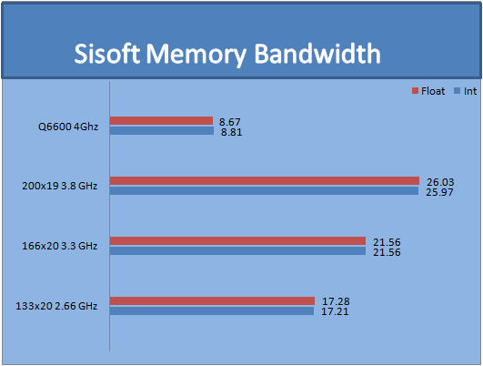
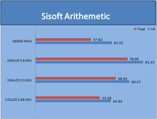

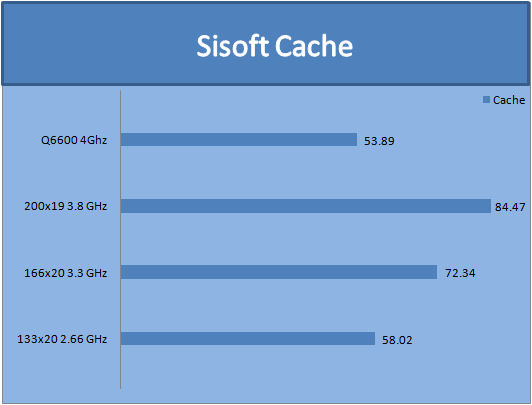
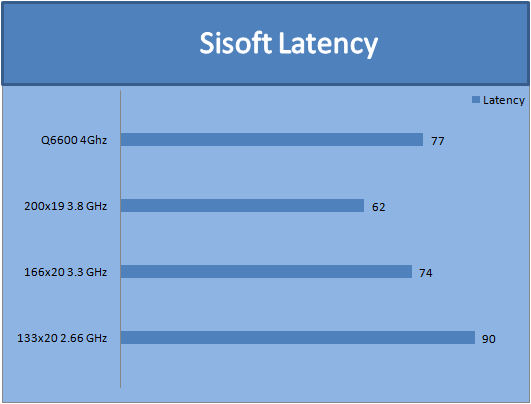
We can see that during SiSoft benchmarking the Core i7 CPU and Smackover combo clearly dominates the scene here. With the few expections, the 4 GHz Q6600 CPU managed to show its abilites and beat the Corei7 while it was in low frequencies during the Float and Int of MultiMedia testing and the Int of Arithemetic testing. The SiSoft latency test, the Q6600 CPU manged to do a tad better than the stock clock speed of the Core i7 CPU.
Super PI
Super Pi is a program that calculates pi to a specified number of digits after the decimal point up to a maximum of 32 million. The Gauss-Legendre algorithm which is a windows version of a program used by Yasumasa Kanada in 1995 to compute Pi to 232 digits.
Super Pi is used by many overclockers to test performance and stability of their systems. In this community, Super Pi has become the standard for providing benchmarks to compare pi calculation times and demonstrate their overclocking skills. The program can be used to also test the stability of a particular overclocking speed. If a computer can calculate PI to the 32 millionth place after the decimal without a mistake, it is considered moderately stable in terms of RAM and CPU performance. More intensive CPU and RAM tests include calculations that run for hours instead of minutes and better test system stress levels.
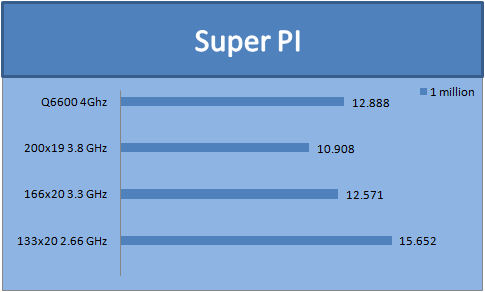
Now, during the Super PI 1m testing the Q6600, did not really stand a chance against the Core i7 CPU. The Q6600 beat the stock clocked Core i7 920 but once the Core i7 came up to 3.3GHz, the old Q6600 CPU couldn’t hang on. Keep in mind this, the Q6600 CPU is cranking at 4GHz at 500MHz x 8 on a GigaByte P45 motherboard.
CineBench
CINEBENCH runs several tests on your computer to measure the performance of the main processor and the graphics card under real world circumstances. The benchmark application makes use of up to 16 CPUs or CPU core.
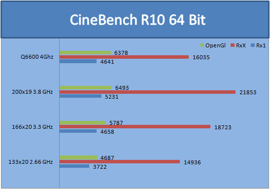
During the CIneBench testing portion we can see that the Smackover X58 motherboard does scale quite nicely once we starting bringing up the FSB of the motherboard.
wPrime
wPrime is a benchmarking application designed to use a highly multithreaded approach to calculating the square-roots of large amounts of numbers (up to 32 billion)

In wPrime testing the Core i7, the extra four threads it has really makes a big difference.
WinRar
WinRar generates random data, which contains specially introduced redundancy, increasing the load to both the processor and memory. Data is then passed through RAR compression and decompression algorithms, and the output of the decompression algorithm is compared to the source data. If any differences are found, WinRAR then reports “Errors found – Yes” in the command window. WinRAR displays a size of processed data and compression speed, current and resulting, in kilobytes per second.
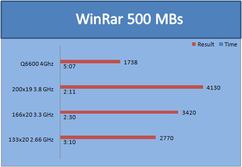
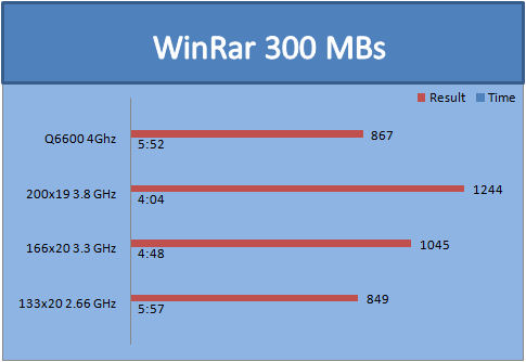
Same principle as I did with the 500 MBs WinRar test but, this time using a single core to calculate the times. This time the Q6600 CPU could manage to keep up with the stock clocked Corei7 CPU, but barely.
EVEREST
EVEREST Ultimate Edition is the cutting-edge benchmarking and diagnostics tool to maximize security, performance, and trouble-shooting capabilities for home and home office PC environments, PC Professionals and consulting firms as well as OEM partners and Configuration Centres worldwide.
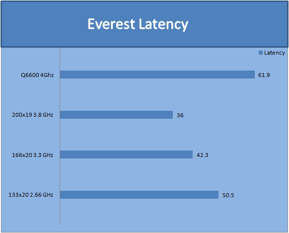
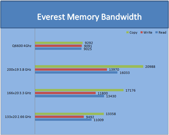
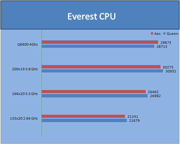
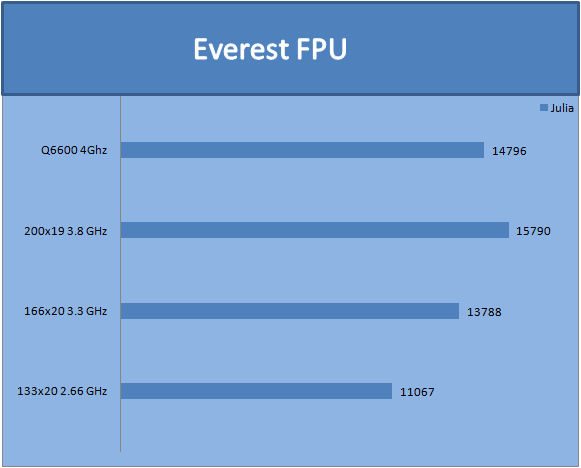
Again, that same pattern we been seeing with the first few tests. The scaling with the Smackover X58 motherboard is consisitant and hasn’t strayed to much up or down. Everest testing kept giving me an error telling me that it was not optimized for my current CPU. So, I take these results with a grain of salt.
3DMARK06

3DMark06 developed by Futuremark, is a synthetic benchmark used for universal testing of all graphics solutions. 3DMark06 features HDR rendering, complex HDR post processing, dynamic soft shadows for all objects, water shader with HDR refraction, HDR reflection, depth fog and Gerstner wave functions, realistic sky model with cloud blending, and approximately 5.4 million triangles and 8.8 million vertices; to name just a few. The measurement unit “3DMark” is intended to give a normalized mean for comparing different GPU/VPUs. It has been accepted as both a standard and a mandatory benchmark throughout the gaming world for measuring performance.

3DMARK VANTAGE

The newest video benchmark from the gang at Futuremark. This utility is still a synthetic benchmark, but one that more closely reflects real world gaming performance. While it is not a perfect replacement for actual game benchmarks, it has its uses. We tested our cards at the ‘Performance’ setting.
Currently, there is a lot of controversy surrounding NVIDIA’s use of a PhysX driver for its 9800 GTX and GTX 200 series cards, thereby putting the ATI brand at a disadvantage. Whereby installing the PyhsX driver, 3DMark Vantage uses the GPU to perform PhysX calculations during a CPU test, and this is where things get a bit gray. If you look at the Driver Approval Policy for 3DMark Vantage it states; “Based on the specification and design of the CPU tests, GPU make, type or driver version may not have a significant effect on the results of either of the CPU tests as indicated in Section 7.3 of the 3DMark Vantage specification and white paper.” Did NVIDIA cheat by having the GPU handle the PhysX calculations or are they perfectly within their right since they own Ageia and all their IP? I think this point will quickly become moot once Futuremark releases an update to the test.
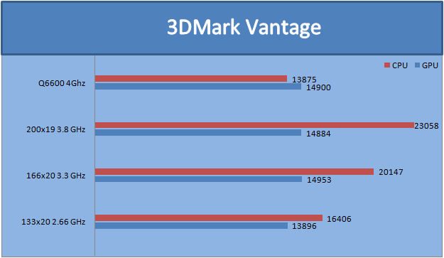
This is the first time I have actually seen a CPU score higher than my GPU score with Vantage, giving me the idea that the CPU is no longer bottlenecking the video card. The CPU score kept increasing as I upped the FSB of the Smackover X58 motherboard, but notiice that between 3.3GHz and 3.8GHz the GPU score is almost identical.
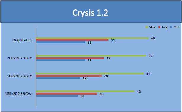
CRYSIS v 1.2
Higher is Better
As always, it doesn’t matter what we do with Crysis, higher CPU speed, better CPU’s, better motherboards, it still runs like crap. The stock Core i7 speed of 2.66MHz scored the worst out of the three Core i7 speeds used.
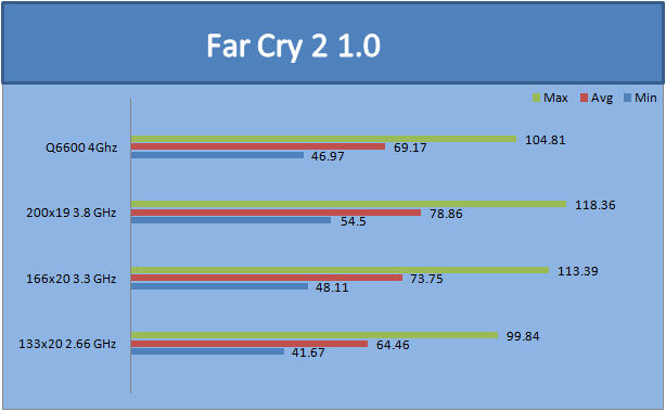
FAR CRY 2
Higher is Better
Now, Far Cry 2, on the other hand actually showed improvement as the CPU speed increased, not much of one, but still it is better than a bump on the head.
CONCLUSIONS
The Smackover X58 motherboard definetly delivers the hype that surrounded it form the rumors we all have been hearing. This motherboard performed beyond my expectations. It also scaled extremely well during overclocking. The overall layout of this motherboard, I will have say, is good (besides the SATA connector placements). The placement of the EPS, 4-pin Molex, and the SATA power plugs were in a great place on the motherboard and would not interfere with other motherboard components, while at the same time allowing us a better way in reagrds to cable management.
Intel finally utilizing some form of a retention plate on the socket 1366 really got my attention. When I was using the stock cooler this little plate made sure the motherboard did not get warped too badly or be bent. Intel should have made this retention plate to include the four CPU mounting holes that surround the CPU socket. I also liked the retention plate’s style that Intel used for the IOH heat sink as well because these bolt holes are spread out far enough apart that when mounting the IOH cooler it would have warped the motheboard here as well.
The only real issues I have with the Smackover X58 motherboard are the SATA ports are at 90 degrees and their close proximity to the video cards will make installing or removing these cables a complete pain, forcing us to to remove the video card(s) every time we need to remove a SATA cable. These should have been 180 degrees.
The use of an onboard power button is a great idea that is being utilized by many manufacturers nowadays. Intel should have also included a reset button as well, as I found my self having to reset the motherboard more often than turning it on and off (luckily I had an extra set of power and reset switches on hand to make this task easier.). Using all solid capacitors would have been a wise choice (this is becoming more and more mainstay with manufacturers), as these will allow the motherboard a longer, more trouble free life span.
Not including PS2 ports isn’t such a bad idea. I realy dont have any negatives to say about this move to eliminating these completly, because 90% of the mice and keyboards are USB anyways. Having a price point on or around the $230 USD mark makes the Intel X58 Smackover a great buy for those who are just starting out with the new Core i7 CPU’s.
Pros:
+Good layout
+BIOS settings are in one place and not scattered
+Good FSB performance scaling
+Retention plate
+Motherboard not cluttered up or clumped together
Cons:
–BIOS sluggish or is combersome when making adjustements or navigating through it
–SATA ports in a bad position
–Does not have all solid capacitors
Final Score: 8.5 out of 10 and the Bjorn3D Seal of Approval
 Bjorn3D.com Bjorn3d.com – Satisfying Your Daily Tech Cravings Since 1996
